VBTA3615M: A Domestic Precision Solution for Compact Signal Switching, the Superior 2N7002KV-TP Alternative
Driven by the demands for miniaturization, high reliability, and supply chain resilience in modern electronics, the substitution of core signal-level MOSFETs has become a strategic focus. Facing the need for efficient voltage control and robust signal switching in compact applications, finding a domestic alternative that offers enhanced performance, consistent quality, and secure supply is crucial for designers. When considering the established 60V dual N-channel MOSFET from MCC—the 2N7002KV-TP—the VBTA3615M, introduced by VBsemi, stands out as a powerful contender. It achieves precise functional compatibility while delivering key performance improvements based on advanced Trench technology, representing a shift from "direct replacement" to "performance enhancement."
I. Parameter Comparison and Performance Enhancement: Core Advantages of Trench Technology
The 2N7002KV-TP has been widely adopted for signal switching and interface protection due to its 60V drain-source voltage, 340mA continuous current, and 5Ω on-state resistance (at VGS=10V). However, its relatively higher RDS(on) can lead to increased conduction losses in space-constrained, efficiency-sensitive designs.
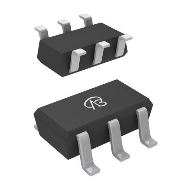
1. Building on hardware compatibility with the same 60V VDS, Dual-N+N configuration, and a compact SC75-6 package, the VBTA3615M achieves notable improvements in key electrical parameters through advanced Trench technology:
Significantly Reduced On-Resistance: With VGS = 10V, the RDS(on) is as low as 1.2Ω, a dramatic reduction of over 75% compared to the reference model. This lower resistance minimizes conduction losses (Pcond = I_D^2⋅RDS(on)) during switching, improving efficiency and thermal performance in low-voltage signal-path applications.
2. Optimized Threshold Voltage & Gate Control: With a standard Vth of 1.7V and a VGS rating of ±20V, the device ensures robust and reliable turn-on/off with common logic-level and microcontroller signals, offering strong noise immunity and control stability.
3. Enhanced Ruggedness & Environmental Compliance: The VBTA3615M maintains high ESD protection (2kV HBM), is halogen-free, and complies with RoHS standards, matching or exceeding the environmental and reliability specs of the original part.
II. Expanding Application Scenarios: From Pin-to-Pin Replacement to Performance Boost
The VBTA3615M enables direct drop-in replacement in existing 2N7002KV-TP footprints while offering system-level benefits:
1. Signal Switching & Level Translation
Lower RDS(on) reduces voltage drop across the switch, improving signal integrity and enabling cleaner level shifting in communication interfaces (I2C, SPI, UART) and GPIO expansion circuits.
2. Load Switching & Power Management
In portable devices, IoT modules, and consumer electronics, its efficiency gains contribute to longer battery life. The compact SC75-6 package is ideal for high-density PCB designs.
3. Protection & Interface Circuits
Used as a high-side or low-side switch for USB ports, sensor power rails, or peripheral enabling, its low on-resistance ensures minimal impact on the powered circuit while providing robust overvoltage protection with its 60V rating.
4. Automotive & Industrial Control Systems
Suitable for non-critical automotive logic, HVAC controls, and PLC I/O modules where 60V robustness, dual-channel design, and stable performance under varying temperatures are required.
III. Beyond Specifications: Supply Chain Assurance and Total Cost Benefits
Choosing the VBTA3615M is a decision that balances technical performance with strategic supply chain advantages:
1. Domestic and Stable Supply
VBsemi controls the design-to-shipment process, ensuring availability, shorter lead times, and resilience against global supply disruptions, providing OEMs and EMS partners with planning security.
2. Cost-Efficiency without Compromise
Offering superior electrical characteristics at a competitive price point, the VBTA3615M reduces the Bill-of-Materials (BOM) cost while enhancing end-product performance and value.
3. Localized Engineering Support
Customers gain access to responsive technical assistance for part selection, circuit simulation, and validation, accelerating design cycles and troubleshooting.
IV. Replacement Guidance and Implementation Path
For designs currently using or specifying the 2N7002KV-TP, the following steps are recommended for a smooth transition:
1. Electrical Validation
Confirm switching behavior and power dissipation in the target circuit. The lower RDS(on) of the VBTA3615M may allow for reduced gate drive strength or improved thermal margins.
2. Layout and Thermal Assessment
Due to the identical SC75-6 footprint, PCB modifications are unnecessary. The reduced conduction loss may allow for further miniaturization or relaxed thermal design.
3. Reliability and System Testing
Perform standard electrical, thermal, and environmental stress tests to validate long-term reliability in the specific application before full-scale deployment.
Embracing a Future of Optimized Signal Switching
The VBsemi VBTA3615M is more than just a domestic substitute for the 2N7002KV-TP; it is an optimized, high-performance dual MOSFET solution for modern compact electronics. Its significantly lower on-resistance, robust gate control, and high ESD tolerance enable designers to improve efficiency, signal fidelity, and system reliability.
In an era prioritizing both performance and supply chain independence, selecting the VBTA3615M is a strategic choice for technological advancement and component security. We confidently recommend this component and look forward to partnering with you to enhance your next-generation electronic designs.


 Download now
 中文
中文 English
 Back to previous page


