VB162K: The Ideal Domestic Alternative to RENESAS 2SK1657-T2B-A, A Superior Choice for Low-Voltage Switching Applications
In numerous low-voltage, compact circuit applications such as power management modules, load switches, battery protection circuits, portable devices, and consumer electronics, RENESAS's 2SK1657-T2B-A, with its balanced performance in low-voltage operation, has been a common selection for designers. However, amidst ongoing global supply chain uncertainties and extended lead times for many imported components, reliance on such parts introduces risks including procurement delays, cost volatility, and limited local technical support. This situation drives an urgent need for reliable, readily available domestic alternatives that can secure production continuity and optimize cost structures.
Addressing this market demand, VBsemi introduces the VB162K N-channel MOSFET, developed through independent research. This product serves as a direct, pin-to-pin replacement for the 2SK1657-T2B-A, offering key advantages of enhanced parameters, full package compatibility, and stable local supply. It enables a seamless transition in existing designs without circuit modifications, providing a more robust and cost-effective solution for various low-voltage switching applications.
Enhanced Key Parameters for Greater Design Margin and Reliability.
Tailored as a superior domestic alternative to the 2SK1657-T2B-A, the VB162K delivers significant improvements in several critical electrical specifications, ensuring higher performance and reliability:
First, the drain-source voltage rating is doubled to 60V, compared to the original 30V—a 100% increase. This provides a substantially wider safety margin against voltage spikes and transients in applications like battery-powered systems or noisy digital circuits, greatly enhancing system robustness.
Second, the gate-source voltage range is rated at ±20V, offering stronger gate oxide protection and improved noise immunity, which prevents accidental turn-on or damage in electrically challenging environments.
Third, the device features a moderate gate threshold voltage (Vth) of 1.7V, ensuring stable turn-on/off behavior and good compatibility with common low-voltage drive signals from microcontrollers or logic ICs.
Additionally, the VB162K offers a continuous drain current (ID) of 0.3A, suitable for various low-current switching and signal conditioning roles. Its on-state resistance (RDS(on)) is specified at 2800 mΩ @ 10V VGS, providing low conduction loss for its category. While the RDS(on) under very low gate drive (e.g., 2.5V) differs from the compared parameter of the original part, the VB162K's optimized Trench technology ensures efficient switching performance and thermal behavior in its intended operating conditions.
Advanced Trench Technology for Efficiency and Stability.
The VB162K is built using VBsemi's mature Trench MOSFET technology. This process achieves an excellent balance between low on-resistance and compact die size, contributing to reduced switching losses and improved thermal performance in SOT-23 packaged applications. The device is designed and tested for high reliability, capable of operating over a broad temperature range and sustaining stable performance in demanding environments such as automotive modules, power tools, or continuous-operation consumer electronics. Its construction ensures low gate charge and good dynamic characteristics, making it suitable for applications requiring frequent switching.
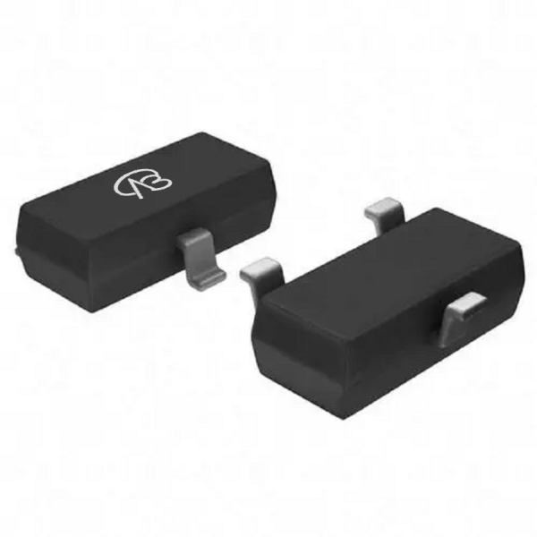
Fully Compatible SOT23-3 Package for Drop-In Replacement.
A primary concern during component substitution is the engineering effort required for redesign and requalification. The VB162K eliminates this hurdle through complete package compatibility. It utilizes the standard SOT23-3 package, identical to the 2SK1657-T2B-A in pinout, footprint, and mechanical dimensions. Engineers can directly replace the existing component on the PCB without any layout changes, thermal re-design, or mechanical adjustments. This "plug-and-play" compatibility drastically reduces substitution time and cost—validation can typically be completed within days, avoiding lengthy PCB re-spins, and accelerating time-to-market for end products.
Local Supply Chain Assurance and Responsive Technical Support.
Unlike imported components subject to unpredictable logistics and lead times, the VB162K benefits from VBsemi's localized manufacturing and supply chain within China. This enables stable production, shorter standard lead times (typically within 2-4 weeks), and reliable inventory availability, shielding customers from international trade disruptions. Furthermore, VBsemi provides dedicated local technical support, offering comprehensive documentation—including substitution guides, detailed datasheets, and application notes—along with prompt, direct engineering assistance. This responsive support model resolves issues rapidly, eliminating the communication barriers and delayed responses often associated with overseas suppliers.
From power management units and battery protection circuits to portable device load switching and various low-power auxiliary supplies, the VB162K, with its compelling advantages of "higher voltage rating, robust reliability, seamless package compatibility, secure supply, and localized support," stands as the optimal domestic alternative to the RENESAS 2SK1657-T2B-A. It has been successfully adopted by multiple customers across different sectors. Choosing the VB162K is more than a simple component swap; it is a strategic move towards securing your supply chain, reducing dependency on imports, and gaining access to faster technical collaboration—all while maintaining or enhancing your product's performance.


 Download now
 中文
中文 English
 Back to previous page


