VBK7322: A Domestic Excellence for High-Performance Low-Voltage Power Management, the Superior RENESAS IDT UPA621TT-E1-A Alternative
Driven by the demand for miniaturization, efficiency, and supply chain resilience in portable electronics and low-voltage power systems, the domestic substitution of core semiconductor components has become a strategic necessity. Facing the stringent requirements for low on-resistance, high reliability, and compact form factors in space-constrained applications, finding a domestic alternative that matches or surpasses international benchmarks in performance, quality, and availability is a key task for designers. When focusing on the popular 20V N-channel MOSFET from RENESAS IDT—the UPA621TT-E1-A—the VBK7322, launched by VBsemi, emerges as a powerful and compelling alternative. It not only achieves direct functional compatibility but also delivers significant performance enhancements, representing a shift from "simple replacement" to "value upgrade."
I. Parameter Comparison and Performance Enhancement: Key Advantages of Advanced Trench Technology
The UPA621TT-E1-A has been widely adopted in applications such as load switching, power management IC (PMIC) companion circuits, and battery protection due to its 20V voltage rating, 5A continuous drain current, and 50mΩ typical on-state resistance (at VGS=4.5V). However, the pursuit of lower conduction loss and higher design margin continues.
1. Building on functional compatibility with a similar Single-N configuration, the VBK7322 achieves notable improvements in key specifications through advanced Trench MOSFET technology:
Higher Voltage Rating & Lower On-Resistance: With a VDS of 30V, it offers a greater design safety margin compared to the 20V reference. Crucially, its RDS(on) is specified at a low 23mΩ (at VGS=10V), representing a dramatic reduction compared to the 50mΩ (at VGS=4.5V) of the UPA621TT-E1-A. According to Pcond = I_D^2⋅RDS(on), this translates to significantly lower conduction losses, improving efficiency and reducing thermal stress.
Optimized for Modern Logic Levels: With a standard gate threshold voltage (Vth) of 1.7V and VGS rating of ±20V, it ensures robust and compatible operation with modern 3.3V/5V MCUs and PMICs.
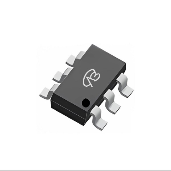
2. Compact Footprint: The SC70-6 package matches the industry-standard small form factor, enabling a true pin-to-pin replacement without board redesign, crucial for space-constrained portable devices.
II. Deepening Application Scenarios: From Direct Replacement to System Optimization
The VBK7322 enables direct replacement in existing UPA621TT-E1-A circuits while offering headroom for system improvement:
1. Load Switching & Power Distribution
Lower RDS(on) minimizes voltage drop and power loss when switching power rails to subsystems (e.g., sensors, peripherals), improving overall system efficiency and battery life in portable devices.
2. Battery Protection & Management Circuits
The 30V rating provides better robustness against voltage spikes. Lower conduction loss reduces heat generation within battery packs, enhancing safety and longevity.
3. PMIC Companion & DC-DC Converter Synchronous Rectification
Suitable as a high-side or low-side switch in low-voltage DC-DC converters. Superior switching performance and low loss contribute to higher converter efficiency.
4. Portable Electronics & IoT Devices
Ideal for smartphones, tablets, wearables, and IoT modules where low quiescent current, high efficiency, and minimal board space are paramount.
III. Beyond Parameters: Reliability, Supply Chain Security, and Full-Lifecycle Value
Choosing the VBK7322 is a decision that balances technical merit with strategic supply chain goals:
1. Domestic Supply Chain Security
VBsemi controls the design, fabrication, and test processes, ensuring a stable, auditable, and predictable supply chain, mitigating risks associated with geopolitical trade tensions.
2. Total Cost Advantage
Offering superior performance at a competitive price point, the VBK7322 reduces the Bill of Materials (BOM) cost while providing potential for system-level savings through simplified thermal management.
3. Localized Technical Support
Access to responsive local engineering support for design-in, validation, and troubleshooting accelerates development cycles and time-to-market.
IV. Adaptation Recommendations and Replacement Path
For designs currently using or specifying the UPA621TT-E1-A, the following evaluation steps are recommended:
1. Electrical Performance Verification
Confirm key parameters under actual operating conditions, especially switching characteristics and losses. The lower RDS(on) of the VBK7322 may allow for efficiency gains or permit operation at slightly higher currents.
2. Thermal and Layout Validation
Due to significantly reduced conduction loss, thermal performance will be improved. Verify that the existing PCB layout and thermal design are adequate or can be optimized further.
3. Reliability and System Testing
Conduct standard reliability tests (electrical stress, temperature cycling, etc.) followed by full system integration testing to ensure long-term stability in the end application.
Advancing Towards Autonomous, High-Efficiency Low-Voltage Design
The VBsemi VBK7322 is more than just a pin-to-pin alternative; it is a superior-performance MOSFET solution for next-generation low-voltage power management. Its advantages in lower on-resistance, higher voltage rating, and compact packaging empower designers to create more efficient, reliable, and competitive electronic products.
In an era prioritizing supply chain diversification and technological sovereignty, selecting the VBK7322 is both a smart engineering choice and a strategic supply chain decision. We confidently recommend this product and look forward to partnering with you to drive innovation in power management design.


 Download now
 中文
中文 English
 Back to previous page


