Breaking Through and Surpassing: How Domestic Dual MOSFET VBC8338 Achieves High-Performance Substitution for VISHAY SI6562CDQ-T1-BE3
Introduction
Dual MOSFETs, integrating both N‑channel and P‑channel devices, are key components in modern power management circuits such as load switches and DC‑DC converters. For years, international brands like VISHAY have set the benchmark with products such as the SI6562CDQ-T1-BE3. However, supply‑chain uncertainties and the pursuit of technological independence have made finding reliable, high‑performance domestic alternatives a strategic priority. Represented by VBsemi’s VBC8338, domestic solutions are now achieving direct对标and even surpassing international classics.
Part 1: Analysis of the Classic Component
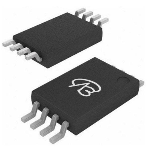
VISHAY’s SI6562CDQ-T1-BE3 is a dual MOSFET (1 N‑channel + 1 P‑channel) in a space‑saving TSSOP‑8 package. It features a drain‑source voltage of 20 V, continuous drain current of 6.7 A, and low on‑resistance of 36 mΩ (at 2.5 V). Its LITTLE FOOT TSSOP‑8 design reduces board footprint and height (1.1 mm) while maintaining good thermal performance, making it suitable for compact power‑switching and converter applications.
Part 2: Performance Surpassing by the Domestic Challenger
VBsemi’s VBC8338 directly对标s the SI6562CDQ-T1-BE3 and delivers notable enhancements in critical parameters:
Higher Voltage Rating: Drain‑source voltage reaches ±30 V (versus 20 V), offering a wider safety margin and greater design flexibility.
Lower Conduction Loss: With on‑resistance as low as 22 mΩ (at 4.5 V) and 45 mΩ (at 10 V), it reduces conduction losses and improves system efficiency.
Full Package Compatibility: Uses the same TSSOP‑8 footprint, enabling drop‑in replacement without layout changes.
Advanced Trench Technology: The device is built on an optimized trench process, ensuring robust performance and reliability.
Part 3: Core Value Beyond Specifications
Selecting a domestic alternative provides deeper strategic benefits:
Supply‑Chain Resilience: Reduces reliance on single‑source international suppliers, ensuring stable supply and production continuity.
Cost Optimization: Typically offers better cost‑effectiveness with equivalent or superior performance, potentially lowering total system cost.
Local Technical Support: Domestic suppliers can provide faster, more responsive engineering support and customized solutions.
Strengthening the Industrial Ecosystem: Every successful adoption helps accumulate experience and drive technological iteration in the domestic semiconductor industry.
Part 4: A Robust Path for Substitution Implementation
To ensure a smooth transition, the following steps are recommended:
Detailed Parameter Comparison: Carefully review all electrical specifications and characteristic curves.
Rigorous Lab Testing: Perform static parameter tests, dynamic switching tests, thermal/efficiency evaluations, and reliability stress tests.
Pilot Verification: Test the component in real‑world applications and monitor long‑term performance.
Develop a Switchover Plan: Implement the substitution gradually after full validation, while keeping the original design as a short‑term backup.
Conclusion: Moving from “Usable” to “Excellent”
The evolution from the SI6562CDQ-T1-BE3 to the VBC8338 demonstrates that domestic dual MOSFETs now possess the capability to compete with and surpass international benchmarks. Adopting such high‑performance domestic components is not only a practical response to supply‑chain challenges, but also a strategic step toward building an autonomous, resilient, and innovative industrial ecosystem. Now is the right time to actively evaluate and adopt high‑quality domestic solutions.


 Download now
 中文
中文 English
 Back to previous page


