VB125N5K: The Optimal Domestic Alternative to TN5325K1-G, A Robust and Supply-Secure Choice for Switching and Amplification Applications
In various switching and amplification applications that demand very low threshold voltage, high breakdown voltage, high input impedance, low input capacitance, and fast switching speed, Microchip Technology's TN5325K1-G, leveraging its vertical DMOS structure and mature silicon gate manufacturing process, has been a reliable choice for engineers by combining the power handling capability of bipolar transistors with the inherent high input impedance and positive temperature coefficient of MOS devices. However, in the current climate of global supply chain volatility and trade uncertainties, sourcing this imported component presents challenges such as extended lead times, cost vulnerabilities, and limited local support. This has propelled the shift towards domestic substitution from a strategic consideration to an operational imperative for ensuring design stability, cost efficiency, and supply chain resilience.
Addressing this critical industry need, VBsemi, through its dedicated R&D in power semiconductors, introduces the VB125N5K N-channel MOSFET. This product is meticulously designed to serve as a direct, pin-to-pin alternative to the TN5325K1-G, offering key advantages of parameter suitability, technological robustness, and full package compatibility. It enables a seamless replacement in existing circuits without modifications, delivering a more accessible, cost-effective, and locally supported solution for a wide range of electronic systems.
Precision-Tuned Parameters with Enhanced Current Capability for Demanding Circuits
Engineered as a domestic counterpart to the TN5325K1-G, the VB125N5K provides a balanced and capable parameter set that meets or exceeds the requirements of targeted applications:
It maintains the same 250V drain-source voltage (Vdss), ensuring equivalent robustness against voltage stresses in circuits designed for this breakdown level. The continuous drain current (Id) is rated at 0.3A, which is double the 150mA of the TN5325K1-G. This 100% increase in current-handling capability offers significant headroom for designs, enhancing system reliability and allowing for potential margin in power handling.
The on-state resistance (RDS(on)) is specified at 1500mΩ (1.5Ω) @ 10V gate drive. While the absolute value is different, this parameter, combined with the higher current rating, is optimized within the device's technology to provide efficient performance in its target application space. The device supports a ±20V gate-source voltage (VGS), ensuring strong gate reliability and noise immunity. A standard 3V gate threshold voltage (Vth) facilitates easy drive compatibility with common logic-level or standard driver ICs, ensuring straightforward integration without drive circuit redesign.
Advanced Trench Technology for Reliable Performance and Intrinsic Safety
The TN5325K1-G capitalizes on the benefits of vertical DMOS and silicon gate technology. The VB125N5K employs modern Trench technology to achieve excellent switching characteristics and high input impedance. This MOS structure inherently avoids issues like thermal runaway and secondary breakdown, ensuring stable operation under varying temperature conditions.
The device is designed for fast switching speeds, making it suitable for high-frequency applications. Its low input capacitance contributes to reduced switching losses and improved efficiency. Furthermore, the VB125N5K is characterized by a wide operating temperature range and undergoes rigorous reliability testing, ensuring stable long-term performance in diverse environments, from consumer electronics to industrial control interfaces.
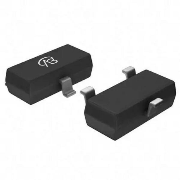
Fully Compatible SOT23-3 Package for effortless Drop-In Replacement
A primary concern in component substitution is the engineering effort required for integration. The VB125N5K eliminates this hurdle through its package design. It is offered in the standard SOT23-3 package, which is physically and dimensionally identical to the package used by the TN5325K1-G. This complete pinout, footprint, and thermal compatibility allows engineers to perform a direct "drop-in" replacement on existing PCB layouts.
This seamless compatibility drastically reduces substitution time and cost: no PCB redesign, no circuit re-simulation for layout effects, and no changes to assembly processes are needed. Validation and testing cycles are shortened significantly, enabling companies to transition to a secure supply source rapidly and with minimal risk.
Localized Supply Chain Assurance and Responsive Technical Support
Unlike imported components subject to international logistics and allocation uncertainties, VBsemi manufactures the VB125N5K within a stable domestic supply chain. With modern production facilities and R&D centers in China, VBsemi guarantees consistent availability, significantly shorter lead times (typically weeks versus potential months), and protection from geopolitical trade disruptions.
As a local supplier, VBsemi provides dedicated, responsive technical support. Customers gain access to comprehensive documentation, including detailed datasheets, application notes, and replacement guides. The technical team offers direct consultation to address any application questions, ensuring a smooth and supported transition from the TN5325K1-G to the VB125N5K.
From low-power switch-mode supplies and signal amplification circuits to various interface driving and protection modules, the VB125N5K stands as the ideal domestic alternative to the Microchip TN5325K1-G. Its combination of suitable electrical parameters, reliable Trench technology, perfect package compatibility, and secure local supply has already led to successful adoption in numerous projects. Choosing the VB125N5K is a strategic step towards securing your supply chain, reducing dependency on volatile imports, and gaining the advantage of local partner support—all without compromising design integrity or performance.


 Download now
 中文
中文 English
 Back to previous page


