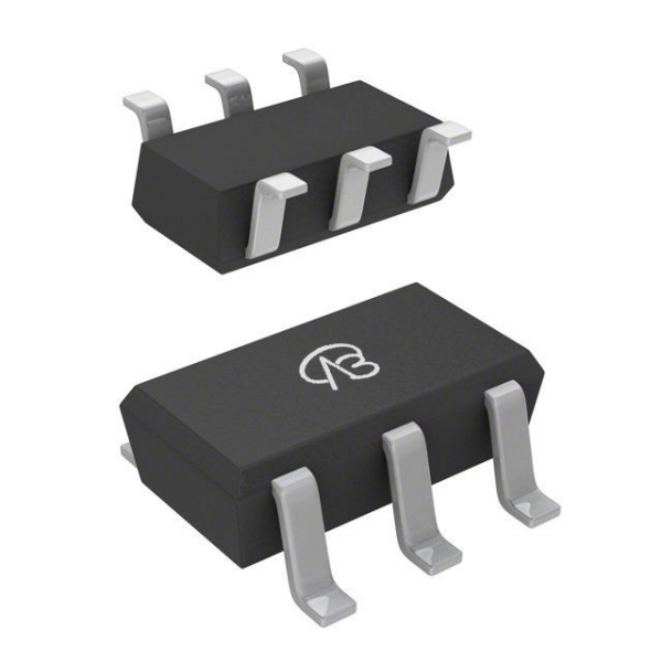
VBTA8338: A Domestic Excellence for Low-Voltage Power Switching, the Superior SSM6J215FE Alternative
In the era of miniaturization and efficiency-driven electronics, the demand for reliable, high-performance power switches in portable devices, battery management, and IoT applications is ever-increasing. Faced with global supply chain uncertainties, domestic substitution of core components has become a strategic necessity for ensuring production continuity and cost competitiveness. When considering the widely used P-channel MOSFET from Toshiba—the SSM6J215FE(TE85L,F)—the VBTA8338, introduced by VBsemi, stands out as a compelling alternative. It not only matches functional compatibility but also delivers enhanced performance through advanced trench technology, transitioning from a mere replacement to a superior solution.
I. Parameter Comparison and Performance Leap: Key Advantages from Trench Technology
The SSM6J215FE(TE85L,F) has gained popularity in low-voltage applications due to its 20V drain-source voltage, 3.4A continuous drain current, and 59mΩ on-state resistance at VGS=4.5V. However, as systems push for higher efficiency and compact designs, lower conduction losses and better switching characteristics are critical.
1.Building on hardware compatibility with a similar SC75-6 package and P-channel configuration, the VBTA8338 achieves notable improvements through optimized trench technology:
Enhanced Voltage Rating and Lower On-Resistance: With a VDS of -30V (surpassing the 20V rating), it offers greater margin for overvoltage scenarios. At VGS=10V, the RDS(on) is as low as 32mΩ, significantly lower than the reference model’s 59mΩ at 4.5V. This reduction directly cuts conduction losses (Pcond = I_D^2⋅RDS(on)), improving efficiency and thermal performance in applications like load switching and DC-DC conversion.
2.Superior Gate-Source Voltage Range: The VBTA8338 supports a VGS of ±20V, providing robust gate driving flexibility and protection against voltage spikes, which enhances system reliability in dynamic environments.
3.Optimized Threshold Voltage: With a Vth of -1.7V, it ensures reliable turn-on and turn-off behavior, reducing the risk of false triggering in noise-sensitive circuits.
II. Deepening Application Scenarios: From Direct Replacement to System Enhancement
The VBTA8338 enables pin-to-pin replacement in existing SSM6J215FE designs while driving system-level upgrades:
1.Battery Management Systems (BMS)
Lower RDS(on) minimizes voltage drop and power loss during charging/discharging, extending battery life and improving efficiency in portable devices and power tools.
2.Load Switches and Power Distribution
In IoT devices and motherboards, the reduced conduction loss allows for cooler operation, enabling higher power density and longer lifespan without heatsink additions.
3.DC-DC Converters (Low-Voltage Buck/Boost)
Enhanced switching performance and low on-resistance support higher efficiency across load ranges, contributing to smaller inductors and capacitors for compact power supplies.
4.Portable Electronics and Consumer Appliances
Suitable for power gating, motor drives in small fans, and LED lighting, where space and thermal constraints are critical, the VBTA8338 delivers reliable performance with its -30V rating and trench technology.
III. Beyond Parameters: Reliability, Supply Chain Security, and Full-Lifecycle Value
Choosing the VBTA8338 is both a technical and strategic decision:
1.Domestic Supply Chain Assurance
VBsemi controls the entire process from chip design to packaging, ensuring stable supply, shorter lead times, and resilience against global trade disruptions, safeguarding production for OEMs and designers.
2.Cost-Effective Performance
With competitive pricing and comparable or better specifications, the VBTA8338 reduces BOM costs while boosting end-product value, ideal for cost-sensitive mass markets.
3.Localized Technical Support
Rapid assistance from selection to failure analysis accelerates design cycles, helping customers optimize layouts and resolve issues quickly, reducing time-to-market.
IV. Adaptation Recommendations and Replacement Path
For designs using or planning to use the SSM6J215FE(TE85L,F), follow these steps for a smooth transition:
1.Electrical Performance Validation
Compare switching waveforms, loss profiles, and efficiency under identical circuit conditions. Leverage the VBTA8338’s low RDS(on) to adjust drive parameters (e.g., VGS) for optimal performance.
2.Thermal and Mechanical Assessment
Due to lower losses, thermal stress may reduce—evaluate opportunities to simplify heatsinking or shrink board space for cost savings.
3.Reliability Testing and System Integration
Conduct environmental, lifespan, and stress tests in labs, followed by field trials in end-devices, to ensure long-term stability and compliance.
Advancing Towards Autonomous, High-Efficiency Power Solutions
The VBsemi VBTA8338 is not just a domestic alternative to international brands; it is a high-performance, reliable MOSFET for next-generation low-voltage power systems. Its advantages in on-resistance, voltage rating, and switching robustness empower customers to achieve gains in efficiency, size reduction, and overall competitiveness.
In a landscape where electronics demand agility and supply chain resilience, opting for the VBTA8338 is a rational move for technological upgrade and strategic autonomy. We highly recommend this product and look forward to partnering with you to innovate and transform power switching applications.


 Download now
 中文
中文 English
 Back to previous page


