VB2610N: A Domestic Excellence for High-Performance Power Management, the Superior SI5618A-TP Alternative
Driven by the dual forces of electronics miniaturization and supply chain resilience, the domestic substitution of core semiconductor devices has evolved from an optional strategy to a critical necessity. Facing the stringent requirements for low on-resistance, high efficiency, and compact size in modern power management applications, finding a domestic alternative that is electrically superior, reliable, and readily available has become a key task for numerous designers. When focusing on the popular 60V P-channel MOSFET from MCC (Micro Commercial Co.) — the SI5618A-TP — the VB2610N, launched by VBsemi, emerges as a formidable contender. It not only achieves direct functional replacement but also realizes a significant leap in key performance parameters, representing a value transformation from "compatible" to "superior," from "substitution" to "upgrade."
I. Parameter Comparison and Performance Leap: Fundamental Advantages of Advanced Trench Technology
The SI5618A-TP has found its place in various load switch and power management circuits due to its -60V voltage rating, -1.6A continuous drain current, and 160mΩ typical on-state resistance. However, as designs push for lower voltage drops and higher power density, its conduction loss and current handling can become limiting factors.
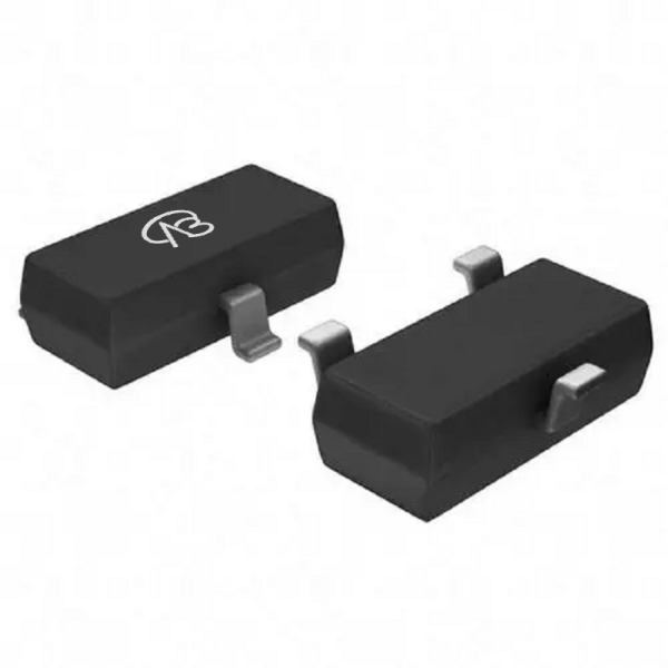
Building on functional compatibility with the same -60V drain-source voltage and SOT23-3 package, the VB2610N achieves remarkable improvements in key electrical characteristics through advanced Trench technology:
1. Drastically Reduced On-Resistance: With VGS = -10V, the RDS(on) is as low as 70mΩ, representing a reduction of over 56% compared to the reference model. According to the conduction loss formula Pcond = I_D^2⋅RDS(on), this translates to significantly lower power dissipation and voltage drop, especially at higher load currents, directly improving system efficiency and thermal performance.
2. Enhanced Current Handling: The continuous drain current rating is boosted to -4.5A, nearly three times that of the SI5618A-TP. This provides a much larger design margin, increases overall system robustness, and allows for the consolidation of components in parallel configurations.
3. Maintained Robustness: The device maintains a ±20V gate-source voltage rating and a similar threshold voltage (Vth ~ -1.7V), ensuring compatibility with standard drive circuits and safe operating areas.
II. Deepening Application Scenarios: From Pin-to-Pin Replacement to Performance Enhancement
The VB2610N enables direct drop-in replacement in existing applications of the SI5618A-TP while offering headroom for system improvement:
1. Load Switching & Power Distribution
Lower RDS(on) minimizes voltage sag and power loss when switching power rails, improving efficiency in battery-powered devices, port power management, and subsystem power gating.
2. DC-DC Converter Protection & Switching
Suitable for input/output protection, reverse polarity protection, and as a low-side switch in synchronous converters. The higher current rating supports higher power stages.
3. Consumer Electronics & Portable Devices
Ideal for space-constrained applications like smartphones, tablets, and wearables where low on-resistance and high efficiency are critical for extending battery life. The SOT23-3 package is perfect for high-density PCB layouts.
4. Industrial Control & Module Power
Provides a reliable and efficient switching solution for low-voltage industrial logic, sensor modules, and communication interfaces.
III. Beyond Parameters: Reliability, Supply Chain Security, and Full-Lifecycle Value
Choosing the VB2610N is a decision that balances technical performance with strategic supply chain benefits:
1. Domestic Supply Chain Security
VBsemi ensures a fully controlled and transparent supply chain from wafer to final test, guaranteeing stable supply and shorter lead times, effectively mitigating risks associated with geopolitical trade uncertainties.
2. Total Cost Advantage
Offering superior electrical performance at a competitive price point, the VB2610N reduces the total cost of ownership and enhances the end product's market competitiveness.
3. Localized Technical Support
Access to rapid, expert-level support for component selection, circuit simulation, and failure analysis accelerates design cycles and problem resolution.
IV. Adaptation Recommendations and Replacement Path
For designs currently using or specifying the SI5618A-TP, the following steps are recommended for a smooth transition:
1. Electrical Performance Validation
Benchmark key parameters such as switching behavior, in-circuit voltage drop, and power dissipation. The superior RDS(on) of the VB2610N may allow for further optimization of thermal management or trace design.
2. Layout and Thermal Consideration
While the package is identical, the lower loss may reduce operating temperature. Verify board-level thermal performance under maximum load conditions to explore potential design optimizations.
3. Reliability and System Validation
Conform to standard qualification procedures including electrical stress, temperature cycling, and long-term reliability tests to ensure robustness in the target application.
Advancing Towards an Autonomous, High-Efficiency Power Management Era
The VBsemi VB2610N is not merely a domestic equivalent to an international brand; it is a high-performance, high-efficiency upgrade for modern low-voltage power switching systems. Its advantages in conduction loss, current capability, and compact form factor empower customers to achieve higher efficiency, greater power density, and improved system reliability.
In an era of increasing electronic integration and supply chain independence, choosing the VB2610N is both a smart technical upgrade and a strategic step towards supply chain resilience. We confidently recommend this product and look forward to partnering with you to drive innovation in power management design.


 Download now
 中文
中文 English
 Back to previous page


