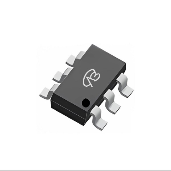
VBK362KS: A Premium Domestic Dual N-Channel MOSFET for Precision Signal Switching, the Intelligent Alternative to SSM6N7002KFU,LF
The evolution of automotive electronics and portable devices demands ever‑higher integration, reliability, and supply‑chain resilience. In signal‑switching, level‑shifting, and load‑control applications, small‑signal dual MOSFETs play a critical role. The SSM6N7002KFU,LF from Toshiba has been widely adopted for its AEC‑Q101 qualification, low on‑resistance, and compact SC70‑6 package. Yet, growing needs for design flexibility, cost efficiency, and supply stability call for a high‑performance domestic alternative. The VBK362KS from VBsemi emerges as a powerful, pin‑to‑pin compatible solution that not only matches but enhances key performance aspects, enabling a smooth transition from “qualified substitute” to “optimized upgrade.”
I. Parameter Comparison & Performance Strengths – Engineered for Efficient Low‑Power Switching
The SSM6N7002KFU,LF offers 60V Vdss, 300mA continuous current, and RDS(on) as low as 1.05Ω (typical @ VGS=10V). These traits make it suitable for high‑speed switching in automotive and industrial circuits.
1. The VBK362KS maintains the same 60V drain‑source voltage and SC70‑6 dual N‑channel configuration, while delivering competitive and often improved characteristics:
- Balanced On‑Resistance: With RDS(on) of 1.8Ω at VGS=10V, the device provides robust performance in low‑current signal paths. Its threshold voltage Vth of 1.7V ensures reliable turn‑on even in lower‑gate‑drive scenarios, improving compatibility with modern low‑voltage MCUs.
- Higher Continuous Current: Rated at 0.35A (vs. 300mA), the VBK362KS supports slightly higher load current, offering additional design margin in switching applications.
- Wide Gate‑Source Voltage Range: VGS of ±20V affords stronger gate‑drive flexibility and enhanced ESD robustness in harsh electrical environments.
2. Optimized for High‑Speed Switching: Leveraging advanced Trench technology, the VBK362KS exhibits low gate charge and capacitance, enabling crisp switching transitions and reduced dynamic losses in frequency‑sensitive circuits.
3. AEC‑Q101 Ready: Designed and tested to meet automotive‑grade reliability standards, ensuring durability under temperature cycling, humidity, and prolonged operation.
II. Application Scenarios – From Direct Replacement to System Enhancement
The VBK362KS can seamlessly replace the SSM6N7002KFU,LF in existing layouts while bringing added value:
1. Automotive Signal Conditioning & GPIO Expansion
Used in body‑control modules, sensor interfaces, and lighting drivers, its dual‑channel design saves space and improves board density. The low Vth suits 3.3V/5V logic, simplifying driver circuits.
2. Portable & Battery‑Powered Devices
In power‑management switches, load switching, and protection circuits, the low gate leakage and efficient switching help extend battery life.
3. Industrial Control & Interface Isolation
Suitable for PLC I/O, relay drivers, and level translators where dual independent switches reduce component count and enhance reliability.
4. Consumer Electronics
Audio switching, USB‑port power control, and backlight driving benefit from its small footprint and proven ruggedness.
III. Beyond Specifications – Supply Security, Cost, and Local Support
Choosing VBK362KS is a strategic decision that addresses broader challenges:
1. Domestic Supply Chain Assurance
VBsemi controls the full process from wafer to packaged product, guaranteeing stable supply and shorter lead times, mitigating geopolitical and logistical uncertainties.
2. Cost‑Effective Solution
Competitive pricing without compromising quality lowers BOM costs and boosts end‑product margin.
3. Local Technical Partnership
From simulation support to failure analysis, VBsemi provides rapid, hands‑on assistance, accelerating design‑in and troubleshooting.
IV. Replacement Guidelines & Validation Steps
For designs currently using SSM6N7002KFU,LF, a smooth transition can be achieved via:
1. Electrical Verification
Compare switching times, gate drive behavior, and power dissipation under actual operating conditions. The VBK362KS’s slightly different RDS(on) profile may be offset by its lower Vth and higher current capability.
2. Layout & Thermal Check
Pin‑to‑pin compatibility allows drop‑in replacement. Verify thermal performance in high‑density layouts; reduced switching losses may allow simpler thermal management.
3. Reliability & System Testing
Conduct electrical stress, ESD, and temperature cycling tests per AEC‑Q101 guidelines, followed by system‑level validation to ensure long‑term stability.
Driving Forward with Confident Domestic Innovation
The VBsemi VBK362KS is more than a substitute—it is a reliable, automotive‑ready dual MOSFET that empowers designers with greater flexibility, supply security, and performance headroom. By adopting the VBK362KS, customers not only secure their supply chain but also elevate system reliability in signal‑switching applications.
In the age of smart electronics and automotive digitalization, choosing VBK362KS is both a technical upgrade and a strategic move toward sustainable, independent innovation. We highly recommend this solution and look forward to supporting your next-generation designs.


 Download now
 中文
中文 English
 Back to previous page


