VB2212N: A Domestic Excellence for Low-Voltage Power Management, the Superior FDN308P Alternative
Driven by the dual trends of electronic device miniaturization and supply chain autonomy, the domestic substitution of core power components has evolved from a backup plan to a strategic necessity. In low-voltage power management applications, where high efficiency, small footprint, and reliability are paramount, finding a domestic alternative that delivers superior performance, consistent quality, and stable supply has become a critical task for designers and manufacturers. When focusing on the classic 20V P-channel MOSFET from ON Semiconductor—the FDN308P—the VB2212N, launched by VBsemi, emerges as a formidable contender. It not only achieves precise pin-to-pin compatibility but also realizes a leap in key parameters through advanced Trench technology, representing a value transformation from "usable" to "excellent," from "substitution" to "surpassing."
I. Parameter Comparison and Performance Leap: Fundamental Advantages Brought by Trench Technology
The FDN308P has earned recognition in power management applications due to its 20V voltage rating, 1.5A continuous drain current, and 190mΩ on-state resistance at VGS=2.5V. However, as systems demand lower losses and higher current handling, its performance limits become apparent.
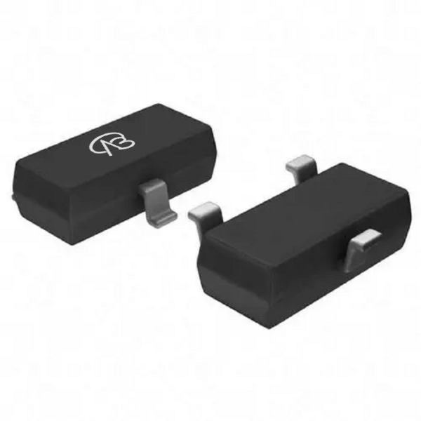
1.Building on hardware compatibility with the same 20V drain-source voltage and SOT23-3 package, the VB2212N achieves significant breakthroughs through advanced Trench technology:
Significantly Reduced On-Resistance: At VGS=10V, the RDS(on) is as low as 71mΩ, a substantial reduction compared to the reference model. According to the conduction loss formula Pcond = I_D^2⋅RDS(on), losses are lower at typical operating currents, directly improving efficiency and reducing thermal stress.
2.Enhanced Current Capability: With a continuous drain current of 3.5A, more than double that of the FDN308P, the VB2212N supports higher-power applications without compromising reliability.
3.Optimized Switching Performance: The Trench technology enables lower gate charge and capacitance, resulting in smaller switching losses under high-frequency operation, thus boosting power density and dynamic response.
4.Wide Gate Drive Range: With a VGS rating of ±12V, the device offers flexibility across various drive voltages, ensuring robust operation in diverse circuit conditions.
II. Deepening Application Scenarios: From Functional Replacement to System Upgrade
The VB2212N not only allows direct replacement in existing FDN308P applications but can also drive overall system improvements with its advantages:
1.Portable Device Power Management: In smartphones, tablets, and wearables, lower conduction losses extend battery life, while the compact SOT23-3 package saves board space.
2.Battery Protection and Load Switching: The high current capability and low RDS(on) minimize voltage drop, enhancing protection accuracy and efficiency in power distribution.
3.DC-DC Converters and Voltage Regulators: The fast switching characteristics support higher frequency designs, reducing the size and cost of passive components like inductors.
4.Industrial and Consumer Electronics: Suitable for low-voltage power supplies, motor drives, and IoT devices, where reliability and efficiency are critical.
III. Beyond Parameters: Reliability, Supply Chain Security, and Full-Lifecycle Value
Choosing the VB2212N is not only a technical decision but also a consideration of supply chain and commercial strategy:
1.Domestic Supply Chain Security: VBsemi possesses controllable capabilities from chip design to packaging, ensuring stable supply, predictable lead times, and mitigation of global trade risks.
2.Comprehensive Cost Advantage: With superior performance, domestic components offer competitive pricing and customization support, reducing BOM costs and enhancing end-product market competitiveness.
3.Localized Technical Support: Provides rapid, full-process support from selection, simulation, testing, to failure analysis, accelerating R&D cycles and problem resolution.
IV. Adaptation Recommendations and Replacement Path
For design projects currently using or planning to use the FDN308P, the following steps are recommended for evaluation and switching:
1.Electrical Performance Verification: Compare key waveforms (switching behavior, loss distribution) under identical circuit conditions. Leverage the VB2212N's low RDS(on) and wide VGS range to optimize drive parameters for efficiency gains.
2.Thermal Design and Mechanical Validation: Due to reduced losses, thermal requirements may be relaxed, allowing potential downsizing of heat sinks or improved reliability in tight spaces.
3.Reliability Testing and System Validation: After completing electrical, thermal, and environmental tests in the lab, proceed to system-level validation to ensure long-term stability in target applications.
Advancing Towards an Autonomous, High-Efficiency Power Management Era
The VBsemi VB2212N is not merely a domestic MOSFET对标ing international brands; it is a high-performance, high-reliability solution for next-generation low-voltage power systems. Its advantages in conduction loss, current capability, and switching performance can help customers achieve comprehensive improvements in system efficiency, power density, and overall competitiveness.
In an era where electronics miniaturization and domestic substitution advance hand-in-hand, choosing the VB2212N is both a rational decision for technological upgrade and a strategic move for supply chain autonomy. We sincerely recommend this product and look forward to collaborating with you to drive innovation and transformation in power management.


 Download now
 中文
中文 English
 Back to previous page


