VBE2610N: The Optimal Domestic Replacement for RENESAS NP15P06SLG-E1-AY in Automotive Low-Voltage Applications
Amidst the global trends of automotive electrification and supply chain diversification, the domestic substitution of foundational power semiconductors has transitioned from a contingency plan to a strategic necessity. For low-voltage, high-current applications demanding robust reliability and efficiency, identifying a capable, quality-assured, and supply-stable domestic alternative is a pressing challenge for automakers and Tier-1 suppliers. Focusing on the widely adopted 60V P-channel MOSFET from RENESAS—the NP15P06SLG-E1-AY—the VBE2610N from VBsemi stands out as a superior replacement. It achieves not only full parametric compatibility but also delivers enhanced performance through advanced trench technology, enabling a value transition from "direct replacement" to "performance upgrade."
I. Parameter Comparison & Performance Enhancement: Key Advantages of Advanced Trench Technology
The RENESAS NP15P06SLG-E1-AY has been a reliable choice for low-side switching, load control, and power management due to its -60V drain-source voltage, -15A continuous current, and 95mΩ typical on-resistance at VGS=-4.5V. However, evolving demands for lower losses and higher power density reveal limitations in its conduction and thermal performance.
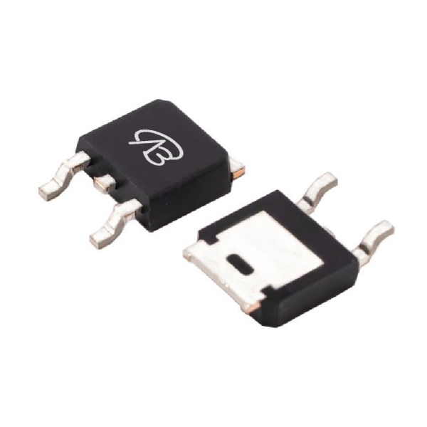
1. Building on hardware compatibility with the same -60V VDS and TO-252 (DPAK) package, the VBE2610N delivers significant improvements in critical electrical parameters via optimized Trench technology:
Reduced On-Resistance: With VGS = -10V, the RDS(on) is as low as 61mΩ, representing approximately a 36% reduction compared to the reference part's 95mΩ@VGS=-4.5V. According to Pcond = I_D^2 · RDS(on), this substantially lowers conduction losses at high currents, improving efficiency and reducing thermal stress.
2. Higher Current Handling: The continuous drain current rating is doubled to -30A, providing greater design margin and reliability for demanding automotive loads, supporting more robust circuit designs.
3. Enhanced Gate Threshold & Drive: With a standard Vth of -1.7V and a VGS rating of ±20V, the device offers good noise immunity and compatibility with common drive circuits, facilitating easier design integration.
II. Application Scenario Expansion: From Pin-to-Pin Replacement to System Optimization
The VBE2610N enables direct drop-in replacement in existing NP15P06SLG-E1-AY designs while offering potential system-level benefits:
1. Automotive Low-Side Switching & Load Control
In body control modules, powertrain auxiliary loads, or LED lighting drivers, lower RDS(on) minimizes voltage drop and power dissipation, enhancing efficiency and enabling more compact layouts.
2. DC-DC Conversion & Power Management
Suitable for secondary-side synchronous rectification or OR-ing circuits in low-voltage DC-DC converters (e.g., 12V/24V systems), where reduced losses contribute to higher efficiency across the load range.
3. Motor Drive & Solenoid Control
For small motors, pumps, or actuator drives in automotive applications, the higher current rating and robust switching performance ensure reliable operation under start-up or stall conditions.
4. Industrial & Consumer Power Systems
In applications like battery protection circuits, hot-swap controllers, or low-voltage UPS, the combination of -60V rating and low RDS(on) provides a reliable and efficient power switching solution.
III. Beyond Specifications: Reliability, Supply Assurance, and Total Cost Benefits
Selecting the VBE2610N is a decision that balances technical performance with strategic supply chain and economic factors:
1. Domestic Supply Chain Resilience
VBsemi maintains full control over design, fabrication, and test processes, ensuring supply stability, predictable lead times, and reduced exposure to geopolitical trade risks, securing production continuity for customers.
2. Total Cost Advantage
Offering comparable or superior performance at a competitive price point, the VBE2610N helps reduce BOM costs while providing potential for system-level savings through relaxed thermal design or component optimization.
3. Localized Technical Support
VBsemi delivers responsive, full-cycle support from component selection and simulation to validation and failure analysis, accelerating design cycles and problem resolution for customers.
IV. Replacement Guidance & Implementation Path
For designs currently using or considering the NP15P06SLG-E1-AY, the following steps are recommended for a smooth transition:
1. Electrical Performance Validation
Compare switching waveforms, loss analysis, and efficiency under identical circuit conditions. The VBE2610N's lower RDS(on) may allow for optimization of drive parameters or layout for further performance gains.
2. Thermal & Mechanical Assessment
Due to reduced conduction losses, thermal dissipation requirements may be lower. Evaluate potential heat sink optimization or PCB layout adjustments for improved reliability or cost savings.
3. Reliability & System-Level Validation
Conduct necessary electrical, thermal, and environmental stress tests in the lab, followed by application-specific system validation to ensure long-term performance and robustness.
Driving Forward with Domestic, High-Performance Power Solutions
The VBsemi VBE2610N is more than a direct functional substitute for the RENESAS NP15P06SLG-E1-AY; it is a enhanced, reliable P-channel MOSFET solution tailored for modern automotive and industrial low-voltage power systems. Its advantages in on-resistance, current capability, and switching robustness empower customers to achieve higher efficiency, greater power density, and improved system reliability.
In an era prioritizing supply chain autonomy and technological advancement, choosing the VBE2610N is both a strategic move for supply security and a technical decision for performance uplift. We confidently recommend this product and look forward to partnering with you to advance the next generation of power electronics solutions.


 Download now
 中文
中文 English
 Back to previous page


