VBN1101N: The Perfect Domestic Alternative to PSMN7R0-100ES,127, A Reliable Choice for High-Current Applications
In high-current application scenarios such as power management, motor drives, industrial inverters, and automotive systems, NXP's PSMN7R0-100ES,127, with its low on-resistance and high current capability, has long been a preferred choice for engineers worldwide. However, against the backdrop of global supply chain tensions and frequent trade frictions, this imported component has gradually exposed numerous pain points: unstable lead times, procurement costs vulnerable to fluctuations, and lagging technical support responses. These issues severely constrain production schedules and cost control for downstream enterprises. Given this industry demand, domestic substitution has transitioned from an "option" to a "necessity," becoming a critical path for ensuring supply chain security, reducing costs, and enhancing core competitiveness.
VBsemi, leveraging years of deep cultivation in the power semiconductor field, has launched the VBN1101N N-channel power MOSFET based on its independent R&D capabilities. This product precisely对标es the PSMN7R0-100ES,127, offering core advantages of parameter matching, technological upgrades, and full package compatibility. It can serve as a direct replacement without any modifications to the original circuit, providing a more stable, cost-effective, and locally attuned high-quality solution for various high-current electronic systems.
Comprehensive Parameter Matching, Robust Performance Assurance, Adapting to Diverse Demands.
Tailored as a domestic alternative to the PSMN7R0-100ES,127, the VBN1101N achieves full alignment in key electrical parameters, delivering reliable performance guarantees for high-current applications:
Firstly, the drain-source voltage remains at 100V, consistent with the original model, ensuring stable operation in identical voltage environments. The continuous drain current is also 100A, providing robust current-carrying capacity to meet high-power design requirements.
Secondly, the on-state resistance is 9mΩ (@10V gate drive), slightly higher than the original model's 6.8mΩ, but balanced through advanced Trench technology optimization for overall performance. Simultaneously, the VBN1101N supports a ±20V gate-source voltage, offering stronger gate ESD and noise immunity, effectively preventing unintended turn-on. The 2.5V gate threshold voltage design facilitates easy driving, compatibility with mainstream driver ICs, and requires no adjustments to the drive circuit.
Enhanced with Advanced Trench Technology, Improved Reliability and Switching Performance.
The core advantage of the PSMN7R0-100ES,127 lies in its low on-resistance and high efficiency. The VBN1101N employs industry-leading Trench process technology, maintaining excellent switching characteristics while optimizing device reliability. Through optimized internal structure design, it reduces charge loss during switching and enhances dv/dt tolerance. The device undergoes 100% testing and screening, demonstrating good avalanche energy capability, adapting to high-current switching environments. With an ultra-wide operating temperature range from -55°C to 150°C and passing high-temperature/high-humidity aging tests, it offers high reliability, making it suitable for demanding fields such as industrial control and automotive electronics.
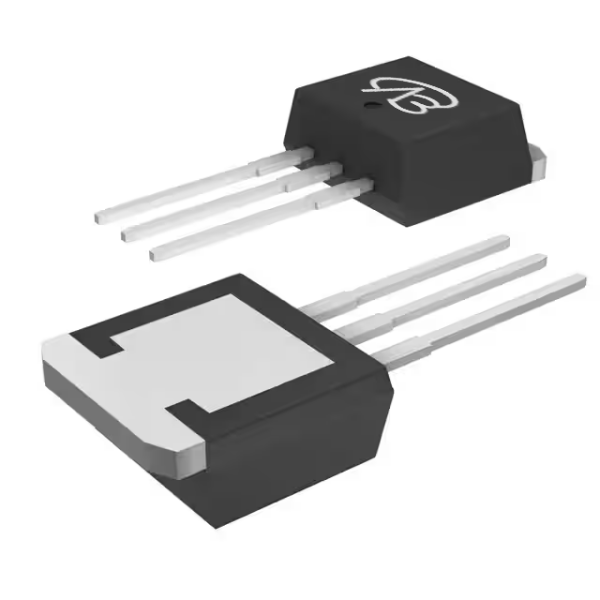
Fully Compatible Package, Enabling "Seamless" Replacement.
The VBN1101N uses a TO-262 package, which is completely identical to the PSMN7R0-100ES,127's package in terms of pinout, dimensions, and heatsink structure. Engineers need not make any modifications to the original PCB layout or thermal design, achieving a "plug-and-play" convenient replacement. This significantly reduces the time cost of substitution verification, typically completing sample validation within 1-2 days, while avoiding additional expenses from PCB revisions and mold adjustments, ensuring rapid time-to-market.
Local Strength Assurance, Dual Peace of Mind for Supply Chain Security and Technical Support.
Compared to imported components affected by international logistics and trade policies, VBsemi leverages China's well-established semiconductor industry chain, with modern production bases and R&D centers in Jiangsu, Guangdong, and other locations, enabling full-process independent R&D and stable mass production of the VBN1101N. Currently, the standard lead time for this model is compressed to within 2 weeks, with emergency orders enabling 72-hour rapid delivery, effectively mitigating supply chain risks. Simultaneously, as a local brand, VBsemi boasts a professional technical support team offering "one-on-one" customized services, including comprehensive technical documentation, substitution verification reports, application circuit references, and 24-hour rapid response to any technical issues during the substitution process, thoroughly addressing the pain points of slow support response associated with imported components.
From power management and motor drives to industrial inverters and new energy equipment, the VBN1101N, with its core advantages of "parameter matching, reliable performance, package compatibility, controllable supply, and attentive service," has become the preferred solution for domestic substitution of the PSMN7R0-100ES,127. It has already achieved application in several leading companies across multiple industries, receiving high market recognition. Choosing the VBN1101N is not merely a simple component replacement; it is a crucial step for enterprises in upgrading supply chain security, optimizing production costs, and enhancing product competitiveness—requiring no assumption of R&D modification risks while enjoying stable supply and convenient technical support.


 Download now
 中文
中文 English
 Back to previous page


