VBN1806: A Domestic Excellence for Medium-Voltage Power Electronics, the Superior 2SK3511-S19-AY Alternative
Driven by the growing demand for efficiency and reliability in power management systems, the domestic substitution of core semiconductor devices has shifted from an alternative choice to a strategic necessity. Facing the requirements for low loss, high current capability, and robust performance in medium-voltage applications, finding a domestic alternative that offers superior performance, reliable quality, and stable supply is crucial for manufacturers across industries. When focusing on the classic 75V N-channel MOSFET from RENESAS IDT—the 2SK3511-S19-AY—the VBN1806, launched by VBsemi, emerges as a powerful contender. It not only achieves precise compatibility but also realizes a significant leap in key parameters based on advanced Trench technology, representing a transformation from "substitution" to "surpassing" in value.
I. Parameter Comparison and Performance Leap: Fundamental Advantages Brought by Trench Technology
The 2SK3511-S19-AY has gained recognition in applications like power supplies and motor drives due to its 75V drain-source voltage, 42A continuous drain current, and 12.5mΩ on-state resistance at VGS=10V. However, as efficiency demands increase and thermal management becomes critical, its conduction losses and current limitations can pose challenges.
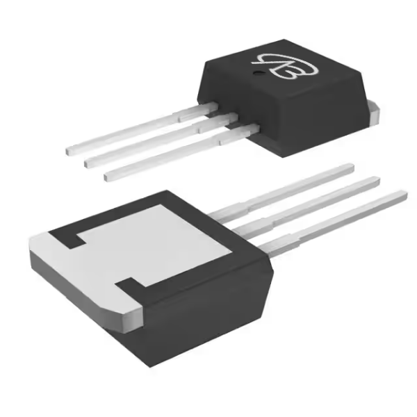
1.Building on hardware compatibility with a similar voltage rating and TO-262 package, the VBN1806 achieves remarkable breakthroughs in electrical characteristics through advanced Trench technology:
Significantly Reduced On-Resistance: With VGS = 10V, the RDS(on) is as low as 6mΩ, a 52% reduction compared to the reference model. According to the conduction loss formula Pcond = I_D^2⋅RDS(on), this drastically lowers losses at high current levels, improving system efficiency, reducing temperature rise, and simplifying thermal design.
2.Enhanced Current Capability: The continuous drain current rating is 85A, more than double that of the 2SK3511-S19-AY, enabling higher power handling and supporting more demanding applications without derating.
3.Optimized Voltage Ratings: With VDS of 80V and VGS of ±20V, it offers robust overvoltage tolerance and gate drive flexibility, ensuring reliability in dynamic operating conditions.
II. Deepening Application Scenarios: From Functional Replacement to System Enhancement
The VBN1806 not only allows pin-to-pin direct replacement in existing designs for the 2SK3511-S19-AY but also drives system-level improvements with its advantages:
1.Switch-Mode Power Supplies (SMPS)
Lower conduction losses enhance efficiency across load ranges, particularly in high-current output stages, enabling compact and energy-efficient designs for servers, telecom, and industrial power systems.
2.Motor Drives and Control Circuits
The high current capability and low RDS(on) support efficient driving of brushed/brushless DC motors in appliances, automotive auxiliary systems, and industrial automation, improving torque response and reducing heat generation.
3.Battery Management and Protection Systems
Suitable for discharge control, load switching, and protection circuits in battery packs for tools, EVs, and energy storage, where low loss and high reliability are critical for longevity and safety.
4. DC-DC Converters and Inverters
In medium-voltage conversion stages, the device’s switching performance and thermal characteristics contribute to higher power density and reliability, ideal for renewable energy and UPS applications.
III. Beyond Parameters: Reliability, Supply Chain Security, and Full-Lifecycle Value
Choosing the VBN1806 is not only a technical upgrade but also a strategic move for supply chain resilience and cost-effectiveness:
1.Domestic Supply Chain Security
VBsemi ensures full-chain control from chip design to packaging and testing, providing stable supply, predictable lead times, and mitigating risks from global trade fluctuations, thus safeguarding production continuity for customers.
2.Comprehensive Cost Advantage
With superior performance at competitive pricing, the VBN1806 reduces BOM costs and offers customization support, enhancing end-product market competitiveness without compromising quality.
3.Localized Technical Support
Rapid, end-to-end assistance from selection and simulation to testing and failure analysis helps customers optimize designs and resolve issues quickly, accelerating development cycles.
IV. Adaptation Recommendations and Replacement Path
For designs currently using or planning to use the 2SK3511-S19-AY, the following steps are recommended for evaluation and switching:
1.Electrical Performance Verification
Compare key waveforms such as switching behavior, loss distribution, and thermal curves under similar circuit conditions. Leverage the low RDS(on) and high current capability of the VBN1806 to fine-tune drive parameters for optimal efficiency.
2.Thermal Design and Mechanical Validation
Due to reduced conduction losses, thermal stress may be lower, allowing potential downsizing of heat sinks or improved reliability in existing layouts. Validate mechanical fit in TO-262 packages.
3.Reliability Testing and System Validation
Conduct thorough electrical, thermal, and environmental stress tests in lab settings, followed by system-level validation to ensure long-term stability in target applications.
Advancing Towards an Autonomous, High-Efficiency Power Electronics Era
The VBsemi VBN1806 is not merely a domestic alternative to international MOSFETs; it is a high-performance, high-reliability solution for next-generation medium-voltage power systems. Its advantages in conduction loss, current handling, and robustness empower customers to achieve superior system efficiency, power density, and overall competitiveness.
In an era of increasing localization and technological advancement, choosing the VBN1806 is both a rational decision for performance upgrade and a strategic step for supply chain autonomy. We highly recommend this product and look forward to collaborating with you to drive innovation in power electronics.


 Download now
 中文
中文 English
 Back to previous page


