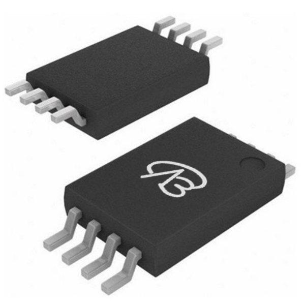
VBC7N3010: A Domestic Excellence for High-Performance Power Electronics, the Superior UPA1808GR-9JG-E1-A Alternative
Driven by the growing demand for efficiency and miniaturization in electronic systems, the domestic substitution of core power devices has evolved from a backup option to a strategic imperative. Facing stringent requirements for low loss, high reliability, and compact design in various applications, finding a domestic alternative solution that is powerful, reliable in quality, and stable in supply has become a critical task for numerous designers and manufacturers. When focusing on the classic 30V N-channel MOSFET from RENESAS IDT—the UPA1808GR-9JG-E1-A—the VBC7N3010, launched by VBsemi, emerges as a formidable contender. It not only achieves precise performance alignment but also realizes a leap forward in key parameters based on advanced Trench technology, representing a value transformation from "usable" to "excellent," from "substitution" to "surpassing."
I. Parameter Comparison and Performance Leap: Fundamental Advantages Brought by Trench Technology
The UPA1808GR-9JG-E1-A has earned recognition in applications like power management and motor drives due to its 30V voltage rating, 9.5A continuous drain current, and 17mΩ on-state resistance at 10V. However, as efficiency demands become more stringent, the inherent losses of the device become bottlenecks.
1. Building on hardware compatibility with the same 30V drain-source voltage and similar package footprint, the VBC7N3010 achieves significant breakthroughs in key electrical characteristics through advanced Trench technology:
Significantly Reduced On-Resistance: With VGS = 10V, the RDS(on) is as low as 12mΩ, a approximately 29% reduction compared to the reference model. According to the conduction loss formula Pcond = I_D^2⋅RDS(on), losses are substantially lower at typical operating currents, directly improving system efficiency and reducing thermal stress.
2. Optimized Switching Performance: Benefiting from Trench structure, the device features lower gate charge and capacitance, enabling faster switching and reduced switching losses in high-frequency applications, thereby enhancing system power density and dynamic response.
3. Robust Operating Characteristics: With a gate-source voltage range of ±20V and a threshold voltage of 1.7V, it offers enhanced drive flexibility and stability, suitable for diverse circuit environments.
II. Deepening Application Scenarios: From Functional Replacement to System Upgrade
The VBC7N3010 not only enables pin-to-pin direct replacement in existing applications of the UPA1808GR-9JG-E1-A but can also drive overall system performance improvements with its advantages:
1. Power Management Modules
Lower conduction losses improve efficiency across load ranges, enabling more compact designs for devices like voltage regulators and load switches.
2. Motor Drives and Control Circuits
Suitable for low-voltage motor drives in consumer electronics, robotics, or automotive auxiliary systems, where reduced losses enhance battery life and thermal management.
3. DC-DC Converters
In step-down or synchronous rectification circuits, the low RDS(on) and fast switching support higher efficiency and frequency, reducing inductor size and cost.
4. Portable and Embedded Systems
Ideal for space-constrained applications due to TSSOP8 packaging and high performance, contributing to longer runtime and smaller form factors.
III. Beyond Parameters: Reliability, Supply Chain Security, and Full-Lifecycle Value
Choosing the VBC7N3010 is not only a technical decision but also a consideration of supply chain and commercial strategy:
1. Domestic Supply Chain Security
VBsemi possesses controllable capabilities across the chain from design to testing, ensuring stable supply, predictable lead times, and mitigation of external risks, safeguarding production continuity for customers.
2. Comprehensive Cost Advantage
With superior performance metrics, domestic components offer competitive pricing and customization support, reducing BOM costs and enhancing end-product market competitiveness.
3. Localized Technical Support
Provides rapid, full-process support from selection to failure analysis, assisting customers with system optimization and troubleshooting, accelerating R&D iteration.
IV. Adaptation Recommendations and Replacement Path
For design projects currently using or planning to use the UPA1808GR-9JG-E1-A, the following steps are recommended for evaluation and switching:
1. Electrical Performance Verification
Compare key waveforms under identical circuit conditions. Utilize the low RDS(on) and optimized switching of the VBC7N3010 to adjust drive parameters for further efficiency gains.
2. Thermal Design and Mechanical Validation
Due to reduced losses, thermal requirements may be relaxed, allowing potential optimization of heat dissipation components for cost or space savings.
3. Reliability Testing and System Validation
After completing electrical, thermal, and environmental tests in the lab, progress to application-specific validation to ensure long-term operational stability.
Advancing Towards an Autonomous, High-Performance Power Electronics Era
The VBsemi VBC7N3010 is not merely a domestic power MOSFET对标ing international brands; it is a high-performance, high-reliability solution for next-generation low-voltage power systems. Its advantages in conduction loss, switching characteristics, and flexibility can help customers achieve comprehensive improvements in system efficiency, power density, and overall competitiveness.
In an era where technological innovation and domestic substitution advance hand-in-hand, choosing the VBC7N3010 is both a rational decision for technological upgrade and a strategic move for supply chain autonomy. We sincerely recommend this product and look forward to collaborating with you to drive innovation and transformation in power electronics.


 Download now
 中文
中文 English
 Back to previous page


