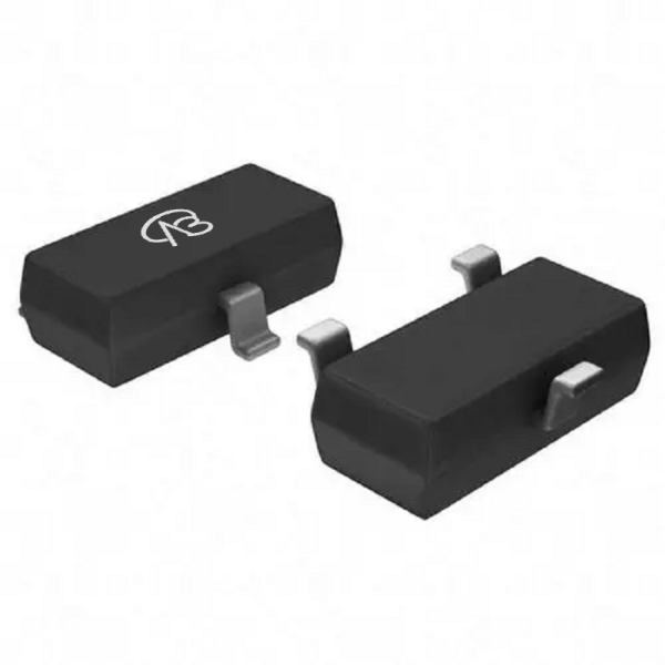
VB1106K: A Premium Domestic Alternative for Small-Signal Switching, Excellently Replacing MCC BSS123-TP
Driven by the trends of device miniaturization and supply chain diversification, the demand for high‑performance, cost‑effective small‑signal MOSFETs in compact electronic designs continues to grow. In applications requiring reliable voltage control and efficient switching, selecting a component that offers low on‑resistance, stable performance, and secure supply has become a key task for designers. Focusing on the widely used 100V N‑channel MOSFET BSS123‑TP from MCC, the VB1106K from VBsemi emerges as a powerful domestic alternative—not only achieving full parameter compatibility but also realizing noticeable performance improvements based on advanced Trench technology, enabling a transition from “direct replacement” to “value upgrade.”
I. Parameter Comparison & Performance Advantages: Enhanced Efficiency with Trench Technology
The MCC BSS123‑TP has been widely adopted in high‑density battery designs and low‑power switching circuits thanks to its 100V drain‑source voltage, 170mA continuous current, and 6Ω on‑resistance (at VGS=10V). However, as designs pursue lower losses and higher current capability, its conduction and current limitations become apparent.
1. While maintaining the same 100V VDS, SOT23‑3 package, and logic‑level compatibility, the VB1106K achieves notable enhancements in key electrical parameters through optimized Trench construction:
- Lower On‑Resistance: At VGS=10V, RDS(on) is only 2.8Ω (typ), less than half that of the BSS123‑TP. This reduction significantly decreases conduction loss in low‑voltage drive scenarios, improving efficiency and thermal performance.
- Higher Current Capability: The continuous drain current reaches 0.26A, about 53% higher than the reference model, allowing for more robust switching in compact designs.
- Favorable Threshold Voltage: With a standard Vth of 1.5V, the device ensures reliable turn‑on/off under low‑drive conditions, compatible with most logic circuits.
2. Improved Switching Dynamics: The low gate charge inherent in Trench technology enables faster switching transitions, reducing dynamic losses in high‑frequency switching applications.
3. Robust & Eco‑Friendly Design: Like the BSS123‑TP, the VB1106K is halogen‑free, RoHS compliant, and features moisture sensitivity level 1 (MSL1), making it suitable for automated assembly and environmentally conscious products.
II. Application Scenarios: Seamless Replacement with Added Value
The VB1106K can directly replace the BSS123‑TP in existing applications while offering headroom for improved performance:
1. Portable & Battery‑Powered Devices
Lower RDS(on) reduces voltage drop across the switch, extending battery runtime in power‑management circuits.
2. Signal Switching & Level Shifting
Enhanced current handling supports stronger drive capability for LEDs, sensors, or small relays in communication modules and interface circuits.
3. Protection Circuits & Load Switching
Suitable for over‑voltage protection, battery isolation, or low‑side switching in power supplies, where lower conduction loss improves overall efficiency.
4. Consumer Electronics & IoT Modules
The SOT23‑3 package and improved performance align with space‑constrained, efficiency‑sensitive designs such as smart wearables, remote controls, and auxiliary power controls.
III. Beyond Specifications: Supply Security, Cost & Support
Choosing VB1106K is both a technical and a strategic decision:
1. Domestic Supply Chain Stability
VBsemi ensures full‑process control from wafer to package, providing stable supply and shorter lead times, reducing dependency on imported components.
2. Cost‑Effectiveness
With superior parameters and competitive pricing, the VB1106K helps lower BOM costs while maintaining or elevating system performance.
3. Local Technical Support
From selection guidance to failure analysis, VBsemi offers responsive, in‑region engineering support, accelerating design‑in and troubleshooting.
IV. Replacement Guidance
For designs currently using or considering the BSS123‑TP, the following steps are recommended:
1. Electrical Verification
Compare switching waveforms and power loss in the target circuit. The lower RDS(on) of VB1106K may allow further optimization of drive conditions.
2. Thermal & Layout Assessment
Reduced conduction loss lowers operating temperature, enabling possible layout simplification or enhanced reliability.
3. Reliability Validation
Perform necessary environmental and life‑cycle tests to confirm long‑term stability under application conditions.
Conclusion: Advancing Compact Design with a Superior Domestic Solution
The VBsemi VB1106K is not merely a pin‑to‑pin alternative to the MCC BSS123‑TP; it is a performance‑enhanced, supply‑secure small‑signal MOSFET that delivers lower resistance, higher current, and better switching efficiency. By adopting the VB1106K, designers can achieve higher system efficiency, improved power handling, and greater supply chain resilience.
In an era emphasizing component miniaturization and supply chain autonomy, choosing VB1106K represents both a smart technical upgrade and a forward‑looking strategic move. We highly recommend this device and look forward to supporting your next‑generation compact electronic designs.


 Download now