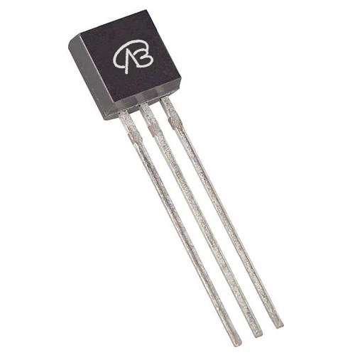
VBR9N602K: A Domestic Precision Alternative for Low-Power Switching, The Superior TN2106N3-G Replacement
Driven by the demand for reliable and cost-effective components in low-power applications, domestic substitution of essential signal and switching devices has become a strategic focus. For circuits requiring low threshold voltage, high input impedance, and efficient switching, finding a domestic alternative that matches or exceeds the performance of established international parts is crucial for design flexibility and supply chain resilience. Focusing on the classic 60V N-channel MOSFET from MICROCHIP—the TN2106N3-G—the VBR9N602K from VBsemi emerges as a precise and enhanced counterpart. It achieves direct functional compatibility while offering superior key electrical parameters, enabling a transition from simple "replacement" to "performance upgrade" in relevant applications.
I. Parameter Comparison & Performance Enhancement: Advantages of Advanced Trench Technology
The TN2106N3-G has been valued for its 60V rating, low threshold, and vertical DMOS structure, offering power handling with high input impedance. However, its conduction resistance presents an opportunity for improvement in efficiency-sensitive designs.
1. Building on foundational compatibility with the same 60V drain-source voltage (VDS) and TO-92 package, the VBR9N602K delivers measurable gains through modern Trench technology:
Reduced On-State Resistance: With VGS = 10V, the RDS(on) is specified at 2000 mΩ (2.0Ω), a 20% improvement over the reference part's typical 2.5Ω. This lower resistance directly minimizes conduction losses (Pcond = I_D^2 RDS(on)) in switching applications, leading to cooler operation and potentially higher efficiency.
2. Optimized for Low-Voltage Drive: With a threshold voltage (Vth) of 0.8V and characterized performance at VGS=4.5V and 10V, the device is exceptionally suitable for low-gate-drive voltage circuits, ensuring robust turn-on in microcontroller-based systems.
3. Inherent MOS Benefits: Like the original part, it retains the desirable characteristics of high input impedance, low input capacitance, fast switching speed, and freedom from thermal runaway, ensuring stable and reliable operation.
II. Application Scenarios: Seamless Replacement and System Benefit
The VBR9N602K is designed for pin-to-pin replacement in existing TN2106N3-G circuits and can enhance performance in various low-power applications:
1. Signal Switching & Amplification
Ideal for analog switches, load switches, and amplification stages where high input impedance and low threshold voltage are critical. The lower RDS(on) reduces signal attenuation and power loss.
2. Consumer Electronics & Peripheral Control
Suitable for power management in portable devices, USB-powered circuits, and peripheral interfacing, where efficiency and thermal performance are constrained by small form factors.
3. Industrial Control & Sensor Modules
Can be used for driving small relays, solenoids, or as a buffer in sensor signal chains, offering reliable switching with minimal drive current requirements.
4. Battery-Powered Applications
The combination of low threshold voltage and improved RDS(on) helps extend battery life in portable equipment by reducing voltage drop and power dissipation in the switch path.
III. Beyond Specifications: Reliability, Supply Assurance, and Added Value
Choosing the VBR9N602K extends beyond electrical parameters into strategic and practical advantages:
1. Domestic Supply Chain Security
Sourcing from VBsemi mitigates risks associated with geopolitical trade tensions and long international lead times, ensuring a stable and responsive supply for production continuity.
2. Cost-Effectiveness
Offers a competitive price point compared to the imported original, reducing Bill of Material (BOM) costs without compromising performance, thereby enhancing end-product market competitiveness.
3. Localized Technical Support
Provides direct access to responsive engineering support for selection, validation, and troubleshooting, accelerating design cycles and problem resolution.
IV. Replacement Guidance
For designs currently using the TN2106N3-G, a smooth transition to the VBR9N602K is recommended:
1. Direct Drop-in Verification
Due to matching electrical characteristics and package (TO-92), the replacement is typically straightforward. Verify key switching waveforms and steady-state temperatures in the target circuit.
2. Drive Optimization (Optional)
The favorable gate characteristics may allow for further optimization of the gate drive circuit or even operation at slightly lower drive voltages in new designs.
3. System Validation
Conduct necessary application-level tests to confirm performance and reliability under real operating conditions.
Embracing Domestic Innovation for Precision Switching
The VBsemi VBR9N602K is not just a functional substitute for the MICROCHIP TN2106N3-G; it is a technically superior choice that leverages advanced Trench technology to deliver lower conduction loss and efficient low-voltage operation. Its compatibility and enhanced parameters make it an ideal solution for upgrading designs requiring reliable, low-power MOSFET performance.
In the pursuit of supply chain diversification and technological independence, adopting the VBR9N602K represents both a prudent technical decision and a strategic move towards greater design autonomy. We confidently recommend this component and look forward to supporting your next innovative design.


 Download now
 中文
中文 English
 Back to previous page


