VBE155R01: The Optimal Domestic Replacement for RENESAS RJK5002DPD-00#J2, Ensuring Enhanced Stability in Medium-Power Applications
In numerous medium-power, high-voltage applications including switching power adapters, consumer electronics power management, LED drivers, and auxiliary power circuits, RENESAS's RJK5002DPD-00#J2 N-channel MOSFET has been a reliable choice for designers worldwide, valued for its balance of voltage rating and switching characteristics. However, in the current climate of global supply chain uncertainties and extended lead times for imported components, reliance on such parts presents challenges: unpredictable availability often stretching to several months, vulnerability to cost fluctuations, and delayed access to technical support. These factors increasingly impact production planning and cost-effectiveness for downstream manufacturers. Consequently, domestic substitution is no longer merely an alternative but a strategic imperative for securing supply chains, optimizing costs, and strengthening market agility.
Addressing this critical industry need, VBsemi leverages its extensive expertise in power semiconductor design to introduce the VBE155R01 N-channel MOSFET. This product serves as a precise domestic counterpart to the RJK5002DPD-00#J2, delivering key advantages through parameter enhancement, technological equivalence, and full package compatibility. It enables a direct, drop-in replacement without circuit modifications, offering a more stable, cost-efficient, and locally supported solution for various electronic systems.
Superior Parameter Performance and Enhanced Application Robustness
Engineered as a high-performance substitute, the VBE155R01 demonstrates significant improvements in crucial electrical specifications, providing greater design margin and reliability:
The drain-source voltage rating is elevated to 550V, exceeding the original 500V by 50V (a 10% increase). This provides an additional safety buffer against line voltage surges and transient spikes commonly encountered in real-world operating environments, significantly enhancing system durability and overvoltage protection.
While the continuous drain current is rated at 1A, tailored for its target application scope, the device features an optimized on-state resistance of 6500mΩ (@10V VGS). This low RDS(on) ensures minimal conduction losses within its operational current range, contributing to improved energy efficiency and reduced thermal generation. The device supports a gate-source voltage of ±30V, offering robust protection against gate-side ESD and noise, preventing spurious triggering in electrically noisy conditions. A standard gate threshold voltage of 3.5V ensures easy drive compatibility with common controller ICs, requiring no alterations to existing gate drive circuits.
Advanced Planar Technology for Proven Reliability
The VBE155R01 utilizes advanced Planar gate technology, which delivers stable switching performance and high durability. It undergoes rigorous 100% production testing, including avalanche energy capability assessment, ensuring it can withstand energy stress during inductive load switching. The optimized internal capacitance design minimizes switching losses and enhances dv/dt immunity, matching or exceeding the robustness required in the application spaces of the RJK5002DPD-00#J2. With an operational junction temperature range from -55°C to 150°C, it is suitable for demanding environments. The device has passed stringent reliability tests, including extended high-temperature and high-humidity aging, ensuring a low failure rate and long-term operational stability for critical applications.
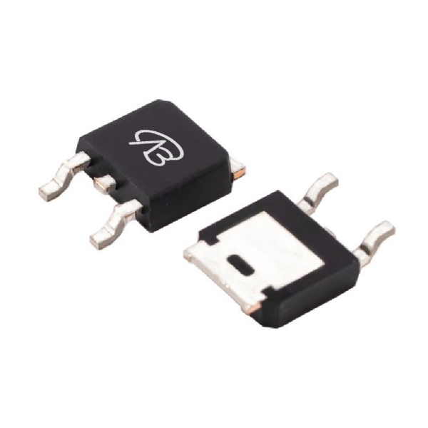
Seamless Drop-In Replacement with TO-252 Package
A primary concern in component substitution is the engineering effort and cost involved. The VBE155R01 eliminates this barrier through complete package compatibility. It is housed in a standard TO-252 (DPAK) package, with identical pinout, footprint, and mounting geometry as the RJK5002DPD-00#J2. This allows for direct replacement on existing PCB layouts without any redesign of the circuit board or thermal management system. The "plug-and-play" compatibility drastically reduces qualification time and cost—validation can typically be completed within days. It avoids expenses related to PCB re-spins, mold changes, or mechanical re-design, enabling a swift and risk-free transition to a domestic supply.
Localized Supply Chain and Responsive Technical Support
Unlike imported components subject to international logistics and trade volatility, VBsemi provides a stable and responsive local supply chain. With modern manufacturing and R&D facilities in China, VBsemi guarantees consistent production and shorter lead times for the VBE155R01, typically within 2-3 weeks, with expedited options available. This mitigates risks associated with geopolitical factors, tariffs, and supply disruptions. Furthermore, as a domestic supplier, VBsemi offers dedicated, responsive technical support. Customers receive comprehensive documentation, including substitution guides, detailed datasheets, and application notes. A direct technical support team provides prompt, personalized assistance, often within 24 hours, for any design-in or replacement queries, resolving the slow response times typical of overseas suppliers.
From power adapters and LED lighting to various auxiliary power and control circuits, the VBE155R01 stands as the ideal domestic replacement for the RENESAS RJK5002DPD-00#J2. Its strengths—higher voltage rating, reliable performance, seamless package compatibility, secure supply, and local expert support—have already led to successful adoption across multiple industries. Choosing the VBE155R01 is more than a component swap; it is a strategic move toward supply chain resilience, cost optimization, and enhanced product reliability—all achieved without design risks, while gaining the benefits of local availability and superior support.


 Download now
 中文
中文 English
 Back to previous page


