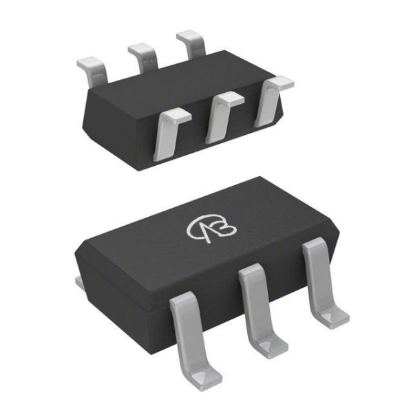
VBTA32S3M: A Domestic Power Solution for Precision Switching, the Superior SSM6N56FE,LM Alternative
Driven by the demand for miniaturization and high efficiency in portable electronics and IoT devices, the need for high-performance, low-voltage MOSFETs with low gate drive requirements has become paramount. Facing design challenges in space-constrained applications requiring efficient power management and signal switching, finding a domestic alternative that offers robust performance, reliable quality, and stable supply is crucial for designers. When focusing on the classic 20V N-channel dual MOSFET from Toshiba—the SSM6N56FE,LM—the VBTA32S3M, launched by VBsemi, emerges as a powerful contender. It not only matches the core functionality but achieves significant enhancements in key electrical parameters, enabling a value transition from "replacement" to "upgrade."
I. Parameter Comparison and Performance Enhancement: Advantages of Advanced Trench Technology
The SSM6N56FE,LM has gained recognition for its ultra-low gate drive capability (down to 1.5V) and dual N-channel configuration in a compact SC75-6 package, making it suitable for low-voltage switching applications. However, its relatively high on-state resistance, especially at lower gate voltages, can limit efficiency and load current handling.
1. Building on fundamental compatibility with the same 20V drain-source voltage and SC75-6 (Dual N+N) package, the VBTA32S3M achieves notable improvements through advanced Trench MOSFET technology:
Superior On-Resistance Consistency: The VBTA32S3M specifies an RDS(on) of 360mΩ (typical per channel) at both VGS = 2.5V and VGS = 4.5V. This represents a significant reduction compared to the SSM6N56FE,LM's specified maximums of 300mΩ @2.5V and 235mΩ @4.5V. More importantly, it offers vastly superior performance at the critical low VGS of 1.5V, where the reference part's RDS(on) rises sharply to 840mΩ (max). This translates to lower conduction losses and reduced voltage drop, especially in low-voltage, battery-powered circuits.
2. Enhanced Current Handling: With a continuous drain current rating of 1A per channel (compared to 800mA), the VBTA32S3M provides greater margin and reliability for load switching, supporting more demanding applications or allowing for downsizing.
3. Flexible Gate Drive: Supporting a VGS range of ±20V and a threshold voltage (Vth) of 0.5-1.5V, it maintains compatibility with very low-voltage logic while offering robustness against gate voltage spikes.
II. Deepening Application Scenarios: From Functional Pin-to-Pin Replacement to System Enhancement
The VBTA32S3M enables direct drop-in replacement in existing designs using the SSM6N56FE,LM while offering potential system-level benefits:
1. Load Switching & Power Management in Portable Devices
In smartphones, tablets, and wearables, its lower RDS(on) at low VGS minimizes power loss when switching power rails for peripherals, sensors, or subsystems, extending battery life. The higher current rating supports the trend of more powerful sub-circuits.
2. Signal Switching and Multiplexing
In audio paths, data lines, or general-purpose digital switching, the low and consistent on-resistance ensures minimal signal attenuation and distortion, improving signal integrity.
3. IoT Modules and Embedded Systems
Its small footprint and efficiency are ideal for space-constrained IoT devices, handling tasks like sensor power cycling, communication module enable/disable, and low-side switching in DC-DC converters.
III. Beyond Parameters: Reliability, Supply Assurance, and Added Value
Choosing the VBTA32S3M is a strategic decision encompassing technical and supply chain factors:
1. Domestic Supply Chain Security
VBsemi's control over design, fabrication, and testing ensures a stable, predictable supply, mitigating risks associated with geopolitical trade fluctuations and ensuring production continuity for customers.
2. Cost-Competitive Advantage
Offering superior electrical characteristics, the VBTA32S3M provides a compelling total cost of ownership, potentially reducing thermal management needs and improving end-product efficiency and reliability.
3. Localized Technical Support
VBsemi provides responsive engineering support throughout the design cycle—from selection and simulation to validation and troubleshooting—accelerating time-to-market.
IV. Adaptation Recommendations and Replacement Path
For designs currently using or considering the SSM6N56FE,LM, the following steps are recommended:
1. Electrical Performance Validation
Verify switching performance and power loss under actual operating conditions. The VBTA32S3M's lower RDS(on) may allow for efficiency gains without circuit modification. Confirm compatibility with existing gate drive levels.
2. Thermal Assessment
Due to reduced conduction losses, thermal performance is expected to improve. This may allow for operation at higher ambient temperatures or simplification of thermal design.
3. Reliability and System Testing
Conduct standard reliability tests (electrical stress, ESD, etc.) followed by system-level validation in the target application to ensure long-term stability and performance.
Advancing Towards Efficient and Autonomous Low-Voltage Design
The VBsemi VBTA32S3M is not just a domestic alternative to an international dual MOSFET; it is a performance-enhanced solution for next-generation low-voltage, high-efficiency switching applications. Its advantages in low-VGS on-resistance, current capability, and consistent performance empower designers to create more efficient, reliable, and compact electronic systems.
In an era prioritizing supply chain resilience and technological innovation, selecting the VBTA32S3M is both a rational engineering choice and a strategic business decision. We confidently recommend this product and look forward to partnering with you to drive innovation in power management and signal switching design.


 Download now
 中文
中文 English
 Back to previous page


