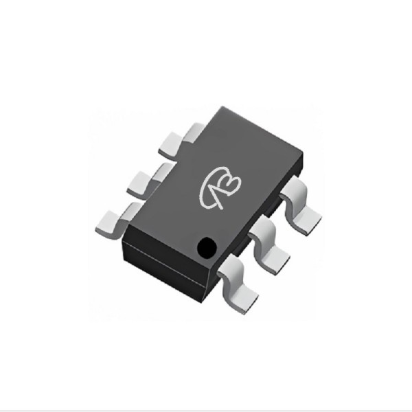
VBK362K: The Domestic Precision Alternative for Compact Signal Switching, Empowering Your Design with Dual-Channel Efficiency
In the realm of compact, low-power signal switching and level translation, efficiency, board space, and reliability are paramount. The MCC BSS138AKDW-TPQ2 has been a popular choice for its SOT-363 (SC70-6) footprint and N-channel logic-level capabilities. However, evolving design demands for higher integration, robust performance, and supply chain diversification call for a superior alternative. The VBsemi VBK362K emerges as a compelling solution, offering a pin-to-pin replacement that not only matches but enhances key specifications with its advanced Trench technology and dual N-channel configuration, transforming your design from "adequate" to "optimized."
I. Parameter Comparison and Performance Enhancement: The Dual-Channel Advantage
The BSS138AKDW-TPQ2 provides a single 50V N-MOSFET with 220mA continuous current and 2Ω typical RDS(on) at VGS=10V. For space-constrained designs requiring multiple switches, this necessitates multiple discrete components.
1. Integrated Dual-Channel Design: The VBK362K integrates two independent N-channel MOSFETs in the same compact SC70-6 package. This effectively doubles functionality without increasing footprint, simplifying PCB layout and reducing component count for applications like dual-load switching or complementary signal paths.
2. Superior Voltage Rating & Robustness: With a higher VDS of 60V and a VGS rating of ±20V, the VBK362K offers greater margin in 12V, 24V, or telecom-based systems, enhancing resilience against voltage spikes and improving overall system reliability.
3. Optimized for Logic-Level Drive: Featuring a low gate threshold voltage (Vth=1.7V) and a low RDS(on) of 2500mΩ (max) at VGS=10V, it ensures efficient switching and minimal conduction loss even when driven directly by 3.3V or 5V microcontrollers, maintaining compatibility with logic-level interfaces.
II. Deepening Application Scenarios: From Simple Switching to Integrated Control
The VBK362K seamlessly replaces the BSS138AKDW-TPQ2 in its existing applications while enabling more integrated and efficient designs:
1. Load Switching & Power Management: Ideal for power gating peripheral circuits, modules, or LEDs in battery-operated devices, IoT sensors, and portable electronics. The dual channels allow independent control of two loads or provide a redundant switch path.
2. Level Translation & Signal Routing: Perfect for I2C, SPI, UART, or GPIO level shifting between different voltage domains (e.g., 1.8V/3.3V/5V). The dual MOSFETs can be configured for bidirectional translation or multi-signal multiplexing.
3. Protection Circuits & Analog Switching: Used in series for current limiting, load disconnect, or as part of analog switch arrays in audio/data acquisition systems, offering low on-resistance and minimal signal distortion.
4. Consumer & Industrial Electronics: Suits a broad range of compact devices such as smartphones, wearables, smart meters, and embedded control boards where space saving and reliable low-power switching are critical.
III. Beyond Parameters: Reliability, Supply Assurance, and Added Value
Selecting the VBK362K is a strategic decision that extends beyond electrical specs:
1. Domestic Supply Chain Security: VBsemi ensures full control from wafer to packaged product, guaranteeing stable supply, shorter lead times, and resilience against global market uncertainties, securing your production lines.
2. Cost and Space Efficiency: The integrated dual-die design reduces the total BOM cost and board area compared to using two discrete SC-70 MOSFETs, offering significant savings in high-volume manufacturing.
3. Localized Technical Support: VBsemi provides rapid, responsive engineering support for device selection, circuit simulation, and validation testing, accelerating your design cycle and troubleshooting process.
IV. Adaptation Recommendations and Replacement Path
For designs currently using or considering the BSS138AKDW-TPQ2, transition to the VBK362K is straightforward:
1. Direct Pin-to-Pin Replacement: The identical SC70-6 package allows a drop-in replacement on existing PCB layouts. Verify the pinout (Dual N+N configuration) matches your circuit schematic.
2. Performance Validation: Test key parameters under actual operating conditions—focus on switching characteristics, leakage current, and thermal performance in your specific application to confirm enhanced margins.
3. System Optimization: Leverage the dual-channel integration to potentially consolidate circuitry, simplify logic control, or add functionality within the same footprint, unlocking further design improvements.
Driving Forward with Compact, Intelligent Power Integration
The VBsemi VBK362K is more than just a domestic alternative; it is an upgraded, integrated solution for modern low-power electronic designs. Its dual-channel architecture, higher voltage robustness, and logic-level compatibility provide a clear path to enhanced performance, reduced size, and greater supply chain stability.
In an era demanding smarter, denser, and more resilient electronics, choosing the VBK362K represents both a technical upgrade and a strategic step towards design optimization and supply chain autonomy. We confidently recommend the VBK362K and look forward to partnering with you to empower your next-generation innovations.


 Download now