VBK162K: The Domestic Precision Upgrade for Signal Switching, The Superior 2N7002W-TP Alternative
Driven by the trends of device miniaturization and supply chain diversification, the demand for reliable, high-performance small-signal MOSFETs in compact electronic designs continues to grow. Facing common requirements for load switching, level shifting, and interface protection in consumer electronics, IoT modules, and portable devices, finding a domestic alternative that offers pin-to-pin compatibility, enhanced performance, and stable supply has become a key task for designers. Focusing on the classic 60V N-channel MOSFET from MCC — the 2N7002W-TP — the VBK162K from VBsemi emerges as a precise and powerful successor. It not only achieves full compatibility but also realizes a performance leap in key parameters, representing a value transition from "direct replacement" to "enhanced upgrade."
I. Parameter Comparison and Performance Enhancement: Core Advantages of Advanced Trench Technology
The 2N7002W-TP has been widely adopted for its 60V drain-source voltage, 115mA continuous current, and 2.5Ω on-resistance (@10V VGS), serving well in low-power switching applications. However, evolving designs demand lower conduction losses and higher current handling in the same footprint.
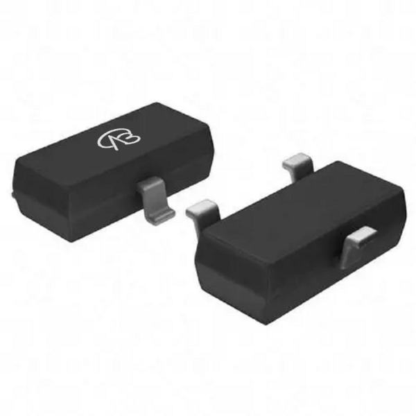
1. Building on hardware compatibility with the same 60V VDS and SC70-3 package, the VBK162K achieves notable improvements through advanced Trench MOSFET technology:
Enhanced Current Capability: The continuous drain current ID is rated at 0.3A, over 2.6 times that of the reference model, providing greater margin and reliability in switching applications.
Reduced On-Resistance: With VGS = 10V, the RDS(on) is specified at 2000mΩ (2.0Ω), a 20% reduction compared to the 2.5Ω of the 2N7002W-TP. This lower RDS(on) minimizes conduction losses, improves efficiency, and reduces heat generation in compact designs.
Optimized Gate Threshold: With a standard Vth of 1.7V, the device ensures robust turn-on with low-voltage logic compatibility, similar to the reference part, facilitating easy design-in.
2. Reliability and Compliance: The VBK162K maintains high reliability standards, featuring a ±20V gate-source voltage rating, suitability for automatic placement, and compliance with RoHS. It aligns with the "green" and halogen-free requirements of modern electronics.
II. Expanded Application Scenarios: From Simple Switching to Robust Performance
The VBK162K enables direct replacement in existing 2N7002W-TP applications while offering headroom for more demanding scenarios:
1. Load Switching & Power Management
In battery-powered devices, its lower RDS(on) and higher current rating reduce voltage drop and power loss when controlling peripherals, sensors, or LED indicators, extending battery life.
2. Level Translation & Interface Protection
Suitable for I2C, SPI, or GPIO level-shifting circuits in mixed-voltage systems (e.g., 3.3V to 5V). The improved current handling offers better robustness against transient loads.
3. Portable & IoT Devices
Ideal for space-constrained applications such as smartphones, wearables, and IoT modules where the SC70-3 package and enhanced efficiency contribute to longer operation and smaller form factors.
4. Consumer Electronics & Module Integration
Can be used in display backlight control, audio mute switches, or USB port power switching, providing reliable performance with a higher safety margin.
III. Beyond Specifications: Supply Chain Stability, Cost, and Support
Choosing the VBK162K is a decision that balances technical performance with strategic supply chain and economic benefits:
1. Domestic Supply Chain Assurance
VBsemi provides full control over design, fabrication, and testing, ensuring stable supply, shorter lead times, and reduced risk from global trade uncertainties, securing production continuity for OEMs and ODMs.
2. Total Cost Advantage
With superior electrical characteristics and competitive pricing, the VBK162K offers a lower total cost of ownership, helping reduce BOM costs while enhancing end-product reliability and performance.
3. Localized Technical Service
VBsemi offers rapid local support for part selection, circuit validation, and failure analysis, accelerating design cycles and problem resolution for customers.
IV. Replacement Guidance and Implementation
For designs currently using or planning to use the 2N7002W-TP, the following steps are recommended for a smooth transition:
1. Electrical Validation
Verify switching behavior and losses in the target circuit. The lower RDS(on) of the VBK162K may allow for reduced drive strength or improved thermal performance.
2. Layout and Thermal Review
The same SC70-3 footprint ensures drop-in compatibility. Due to lower losses, thermal performance may be improved, but standard layout practices for small-signal MOSFETs should be followed.
3. Reliability and System Testing
Conduct standard board-level validation under expected operating conditions to ensure long-term reliability in the application environment.
Stepping into a New Era of Miniaturized and Efficient Power Switching
The VBsemi VBK162K is not just a domestic alternative to the 2N7002W-TP; it is an upgraded solution offering higher current capability, lower on-resistance, and full package compatibility. Its advantages enable designers to improve efficiency, reliability, and power density in space-constrained applications.
In an era prioritizing supply chain resilience and performance optimization, choosing the VBK162K is both a smart engineering upgrade and a strategic move toward supply chain diversification. We highly recommend this component and look forward to partnering with you to drive innovation in compact and efficient electronic designs.


 Download now
 中文
中文 English
 Back to previous page


