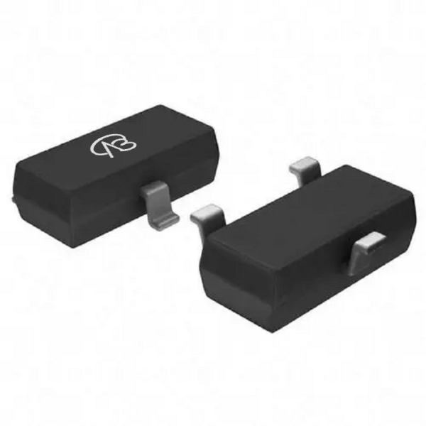
VB162K: A Domestic Excellence for Low-Power Electronic Applications, the Superior 2SK1582-T1B-A Alternative
Driven by the growing demand for component localization and supply chain resilience in the electronics industry, domestic substitution of core semiconductors has shifted from a contingency plan to a strategic priority. For low-power applications requiring reliable switching and efficient performance, finding a domestic alternative that offers competitive specs, stable quality, and secure supply is crucial for designers and manufacturers. Focusing on the classic 30V N-channel MOSFET from RENESAS IDT—the 2SK1582-T1B-A—the VB162K, introduced by VBsemi, stands out as a powerful contender. It not only matches functional compatibility but also achieves a performance leap through advanced Trench technology, transitioning from "drop-in replacement" to "performance upgrade."
I. Parameter Comparison and Performance Leap: Core Advantages Enabled by Trench Technology
The 2SK1582-T1B-A has been widely used in low-voltage circuits due to its 30V drain-source voltage, 200mA continuous drain current, and 5Ω on-state resistance at VGS=4V. However, as designs push for higher efficiency and broader voltage margins, its relatively high RDS(on) and limited current handling can become constraints.
1.Building on hardware compatibility with the same SOT23-3 package and N-channel configuration, the VB162K delivers significant enhancements in key electrical parameters via optimized Trench technology:
Higher Voltage Rating and Current Capacity: With a VDS of 60V (double the reference) and ID of 0.3A (50% higher), it provides greater design headroom for voltage spikes and load variations, improving system robustness in applications like power management or load switching.
2.Reduced On-Resistance: At VGS=10V, the RDS(on) is as low as 2800mΩ (2.8Ω), substantially lower than the 5Ω of the 2SK1582-T1B-A at 4V. Even at comparable gate drive levels, the VB162K’s lower resistance cuts conduction losses per Pcond = I_D^2⋅RDS(on), boosting efficiency and reducing thermal stress in low-power circuits.
3.Enhanced Gate Characteristics: With a Vth of 1.7V and VGS rating of ±20V, it ensures reliable switching and compatibility with modern low-voltage MCUs, while offering wider drive flexibility for noise immunity.
II. Deepening Application Scenarios: From Direct Replacement to System Enhancement
The VB162K enables pin-to-pin replacement in existing 2SK1582-T1B-A designs while unlocking system-level improvements:
1.Power Management and DC-DC Conversion
Ideal for low-power buck/boost converters or LDO alternatives, its lower RDS(on) minimizes dropout losses, extending battery life in portable devices or IoT sensors.
2.Signal Switching and Protection Circuits
Suitable for load switches, multiplexers, or overvoltage protection in consumer electronics, automotive modules, or industrial controls, where higher VDS guards against transients.
3.Audio and Amplifier Output Stages
Can replace MOSFETs in audio switching or small motor drives, offering cleaner switching and better thermal performance due to reduced losses.
4.General-Purpose Low-Power Switching
In relay drivers, LED drivers, or peripheral interfaces, the improved current handling and efficiency support more compact and reliable designs.
III. Beyond Parameters: Reliability, Supply Chain Security, and Full-Lifecycle Value
Choosing the VB162K is both a technical and strategic decision:
1.Domestic Supply Chain Assurance
VBsemi controls the full chain from design to testing, ensuring stable supply, shorter lead times, and resilience against global disruptions, safeguarding production for OEMs.
2.Cost and Customization Edge
With superior specs at competitive pricing, it reduces BOM costs and offers customization options, enhancing end-product value.
3.Local Technical Support
Rapid assistance from selection to failure analysis accelerates development and troubleshooting, fostering faster time-to-market.
IV. Adaptation Recommendations and Replacement Path
For designs using or considering the 2SK1582-T1B-A, follow these steps for a smooth transition:
1.Electrical Validation
Compare switching waveforms, loss profiles, and efficiency under actual circuit conditions. Leverage the VB162K’s lower RDS(on) to optimize gate drive or adjust timing for better performance.
2.Thermal and Mechanical Check
Due to reduced losses, thermal margins may improve, allowing potential downsizing of heatsinks or layout adjustments in space-constrained applications.
3.Reliability and System Testing
Conduct electrical stress, environmental, and lifespan tests in lab settings, followed by field trials to ensure long-term stability in target applications.
Advancing Toward Autonomous, High-Efficiency Low-Power Solutions
The VBsemi VB162K is more than a domestic substitute; it is a high-performance upgrade for low-power electronic systems. Its advantages in voltage rating, on-resistance, and current capacity empower designers to achieve higher efficiency, reliability, and design flexibility.
In an era of increasing localization and performance demands, selecting the VB162K is a rational move for technology enhancement and a strategic step for supply chain independence. We highly recommend this product and look forward to partnering with you to innovate in low-power electronics.


 Download now