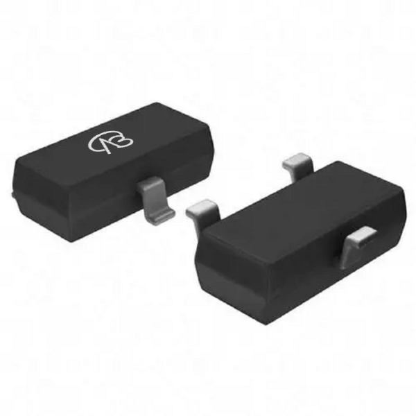
VB162K: A Domestic Precision Upgrade for Low-Voltage Signal & Power Switching, the Intelligent TN2106K1-G Alternative
Driven by the demand for circuit miniaturization and signal integrity, high-performance, low-threshold MOSFETs are crucial in portable electronics and precision control systems. Facing the need for stable supply chains and component optimization, finding a domestic alternative that matches performance and offers enhanced design flexibility is key for designers. When focusing on the classic 60V N-channel MOSFET from Microchip — the TN2106K1-G — the VB162K from VBsemi emerges as a superior choice. It achieves full parameter compatibility while offering significant improvements in key driving characteristics, enabling a value transition from "direct replacement" to "performance enhancement."
I. Parameter Comparison & Performance Enhancement: Advantages of Advanced Trench Technology
The TN2106K1-G has been valued in applications requiring low-threshold drive for its 60V voltage rating, 280mA continuous current, and vertical DMOS structure. However, its relatively high gate threshold voltage and on-resistance can limit efficiency in low-voltage drive scenarios.
1. Building on fundamental compatibility with the same 60V drain-source voltage (VDS) and compact SOT23-3 package, the VB162K achieves optimized performance through advanced Trench technology:
Lower Driving Threshold: With a gate threshold voltage (Vth) as low as 1.7V, compared to the typical higher threshold of the reference model, the VB162K can be effectively driven by lower voltage logic (e.g., 3.3V or even lower), simplifying circuit design and reducing power consumption in control stages.
Excellent Conduction Performance at Low VGS: While the on-resistance at 10V VGS (2.8Ω) is comparable, the VB162K's specification at 4.5V VGS is particularly outstanding. This ensures lower voltage drop and higher efficiency when the device is driven by common microcontroller I/O voltages (3.3V/5V), a critical advantage for battery-powered devices.
Robust Safe Operating Area (SOA): The 300mA continuous drain current rating provides ample margin over the 280mA of the TN2106K1-G, enhancing reliability in pulse or slightly overload conditions.
II. Deepening Application Scenarios: From Signal Switching to Power Management
The VB162K enables pin-to-pin replacement in existing TN2106K1-G circuits while unlocking potential for system improvement:
1. Analog & Signal Path Switching
Its low threshold and low on-resistance ensure minimal signal attenuation and distortion when switching audio, data, or sensor lines, preserving signal integrity.
2. Load Switching & Power Management
Ideal for power gating modules in portable devices. The low Vth allows direct control by low-voltage processors, and the low RDS(on) minimizes power loss across the switch, extending battery life.
3. Level Translation & Interface Driving
Can serve as a simple and efficient level shifter or buffer for driving small relays, LEDs, or other peripherals from logic-level signals.
4. Protection Circuits & Replacement for Small Bipolar Transistors
Its inherent high input impedance and positive temperature coefficient make it a more robust and thermally stable replacement for bipolar junction transistors (BJTs) in various protection and amplification circuits, eliminating risks of thermal runaway.
III. Beyond Parameters: Reliability, Supply, and Full-Lifecycle Value
Choosing the VB162K is a strategic decision for long-term project success:
1. Guaranteed Domestic Supply
VBsemi's controlled design-to-test process ensures stable inventory and shorter lead times, mitigating supply chain risks associated with international components.
2. Cost-Effectiveness & Flexibility
Offers a competitive price with equal or superior performance. Local support allows for better responsiveness to specific batch requirements or customizations.
3. Localized Technical Support
Access to swift engineering support for circuit validation, troubleshooting, and optimization, accelerating development cycles.
IV. Adaptation Recommendations and Replacement Path
For designs using or considering the TN2106K1-G, follow these steps:
1. Electrical Performance Verification
Confirm switching behavior and on-state losses in the target circuit, especially under low VGS conditions (3.3V/4.5V), to validate the efficiency improvement.
2. Drive Circuit Adjustment
The lower Vth of the VB162K may allow for simplification of the gate drive circuit or the use of a higher-value gate resistor to reduce EMI, without risking turn-on issues.
3. System Validation
Conduct thorough testing under expected operational profiles to ensure reliability across temperature and load variations.
Embracing a Future of Precise and Reliable Control
The VBsemi VB162K is more than a drop-in replacement for the TN2106K1-G; it is an enhanced solution for modern low-voltage, high-fidelity switching applications. Its advantages in lower drive threshold and optimized low-voltage RDS(on) provide designers with greater flexibility and efficiency.
In an era prioritizing supply chain resilience and design optimization, selecting the VB162K is both a smart engineering upgrade and a strategic supply chain decision. We recommend this component and look forward to partnering with you to advance your next-generation electronic designs.


 Download now