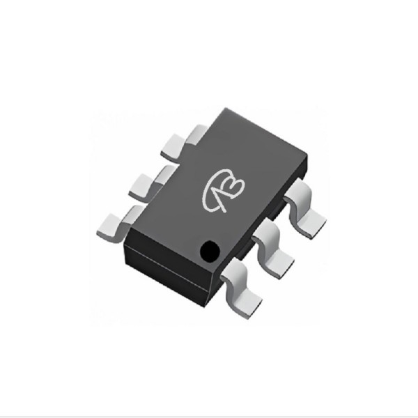
VBK5213N: A Domestic Excellence for High-Efficiency Power Management, the Superior DMC3401LDW-13 Alternative
Driven by the dual forces of demand for miniaturization and heightened efficiency in power systems, the domestic substitution of core power semiconductors has evolved from an alternative choice to a strategic necessity. Facing the stringent requirements for low on-resistance, excellent switching performance, and compact footprint in space-constrained applications, finding a domestic dual MOSFET solution that is performance-competitive, reliable, and supply-stable has become a critical task for numerous designers. When focusing on the classic 30V Dual N+P Channel MOSFET from Diodes Incorporated—the DMC3401LDW-13—the VBK5213N, launched by VBsemi, emerges as a formidable contender. It not only achieves precise functional alignment but also realizes a significant leap in key electrical parameters, representing a value transformation from "compatible" to "enhanced."
I. Parameter Comparison and Performance Leap: Fundamental Advantages of Advanced Trench Technology
The DMC3401LDW-13 has earned recognition in efficient power management applications due to its 30V Vdss rating, 800mA/550mA continuous drain current, and low on-resistance. However, as designs pursue higher efficiency and power density, lower conduction loss and better drive capability become increasingly critical.
1.Building on functional compatibility with the same Dual N+P configuration in a compact package, the VBK5213N achieves remarkable improvements in key electrical characteristics through advanced Trench technology:
Significantly Reduced On-Resistance: With VGS = 4.5V, the RDS(on) for the N-channel is as low as 110mΩ (typ), and for the P-channel is 190mΩ (typ). This represents a reduction of over 70% for the N-channel and nearly 80% for the P-channel compared to the typical RDS(on) of the reference model (400mΩ & 900mΩ @10V). According to the conduction loss formula Pcond = I_D^2⋅RDS(on), this dramatic reduction leads to substantially lower losses at typical operating currents, directly improving system efficiency and thermal performance.
2.Enhanced Current Capability: The VBK5213N supports a continuous drain current (ID) of 3.28A for the N-channel and 2.8A for the P-channel, significantly higher than the 800mA and 550mA of the DMC3401LDW-13. This allows for more robust load handling and provides greater design margin.
3.Optimized for Low-Voltage Operation: With a low gate threshold voltage (Vth) of 1.0-1.2V and excellent RDS(on) performance at low gate drive voltages (e.g., 2.5V and 4.5V), the VBK5213N is perfectly suited for modern low-voltage power rails and battery-powered applications, enabling efficient power switching even in systems with limited gate drive voltage headroom.
II. Deepening Application Scenarios: From Pin-to-Pin Replacement to Performance Upgrade
The VBK5213N not only enables a direct footprint replacement in existing applications of the DMC3401LDW-13 but can also drive overall system performance improvements with its advantages:
1.Load Switches & Power Distribution
Lower conduction loss minimizes voltage drop and heat generation in power path management, improving efficiency and reliability for battery-powered devices, portables, and IoT modules.
2.DC-DC Converter Synchronous Stages
The combination of low RDS(on) and high current capability makes it an excellent choice for synchronous rectification in step-down/step-up converters, enhancing conversion efficiency across the load range.
3.Battery Protection Circuits & Management
The robust performance of both N and P channels supports efficient charging and discharging control in battery packs and management systems, contributing to longer battery life.
4.Signal Level Shifting & Interface Control
The dual complementary channels are ideal for driving and controlling signals in communication interfaces, GPIO expansion, and level translation circuits.
III. Beyond Parameters: Reliability, Supply Chain Security, and Full-Lifecycle Value
Choosing the VBK5213N is not only a technical decision but also a consideration of supply chain and commercial strategy:
1.Domestic Supply Chain Security
VBsemi possesses controllable capabilities across the design and manufacturing chain, ensuring stable supply, predictable lead times, and effectively mitigating risks associated with geopolitical and trade uncertainties.
2.Comprehensive Cost Advantage
With superior performance in key parameters, the VBK5213N offers a highly competitive value proposition, potentially reducing system BOM costs through improved efficiency or allowing for more compact thermal solutions.
3.Localized Technical Support
Provides rapid, responsive support throughout the design cycle—from selection and simulation to testing and failure analysis—accelerating customer time-to-market and problem resolution.
IV. Adaptation Recommendations and Replacement Path
For design projects currently using or planning to use the DMC3401LDW-13, the following steps are recommended for evaluation and switching:
1.Electrical Performance Verification
While the VBK5213N has a slightly lower absolute VDS rating (±20V vs 30V), it is fully suitable for the vast majority of 5V, 3.3V, and 12V rail applications. Verify key waveforms and efficiency under typical operating conditions. The significantly lower RDS(on) will yield immediate efficiency gains.
2.Thermal and Layout Validation
Due to the substantial reduction in conduction losses, thermal stress will be lower. This may allow for optimization of PCB layout or reduction of thermal management overhead. The SC70-6 package maintains a compact footprint.
3.Reliability Testing and System Validation
After confirming electrical performance in the lab, proceed with necessary application-specific stress tests and system-level validation to ensure long-term reliability.
Advancing Towards an Autonomous, High-Performance Power Management Era
The VBsemi VBK5213N is not merely a domestic dual MOSFET对标ing an international brand; it is a high-performance, high-efficiency solution for next-generation power management systems. Its dramatic advantages in on-resistance, current capability, and low-voltage operation can help customers achieve significant improvements in system efficiency, power density, and thermal performance.
In an era where efficiency and miniaturization are paramount, choosing the VBK5213N is both a rational decision for technical upgrade and a strategic move for supply chain resilience. We sincerely recommend this product and look forward to collaborating with you to drive innovation in power electronics design.


 Download now