MOSFET Selection for Compact Power Applications: SI1539CDL-T1-GE3, SIS176LDN-T1-GE3 vs. China Alternatives VBK5213N, VBQF1615
In the pursuit of device miniaturization and high efficiency today, selecting a MOSFET that is 'just right' for a compact circuit board is a practical challenge faced by every engineer. This is not merely completing a substitution from a model list, but a precise trade-off among performance, size, cost, and supply chain resilience. This article will use the two highly representative MOSFETs, SI1539CDL-T1-GE3 (Dual N+P Channel) and SIS176LDN-T1-GE3 (N-channel), as benchmarks, deeply analyze their design cores and application scenarios, and comparatively evaluate the two domestic alternative solutions, VBK5213N and VBQF1615. By clarifying the parameter differences and performance orientations among them, we aim to provide you with a clear selection map, helping you find the most matching power switching solution for your next design in the complex world of components.
Comparative Analysis: SI1539CDL-T1-GE3 (Dual N+P Channel) vs. VBK5213N
Analysis of the Original Model (SI1539CDL-T1-GE3) Core:
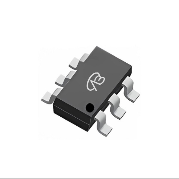
This is a 30V Dual N+P Channel MOSFET from VISHAY, using an ultra-small SC-70-6 (SOT-363) package. Its design core is to provide efficient, compact switching for low-current signal applications. The key advantages are: it integrates one N-channel and one P-channel in one package, suitable for direct or level-shift configuration switching. It features a continuous drain current of 700mA and an on-resistance (RDS(on)) of 1.7Ω at 4.5V gate drive. The SC-70-6 package offers improved thermal performance in a minimal footprint.
Compatibility and Differences of the Domestic Alternative (VBK5213N):
VBsemi's VBK5213N also uses the compact SC70-6 package and is a direct pin-to-pin compatible alternative for dual N+P channel applications. The main differences lie in the electrical parameters: VBK5213N has a slightly lower voltage rating (±20V vs. 30V) but offers significantly superior conduction performance. Its on-resistance is dramatically lower at 90mΩ (N-channel) and 155mΩ (P-channel) @4.5V, and it supports a higher continuous current of 3.28A (N-channel) / -2.8A (P-channel).
Key Application Areas:
Original Model SI1539CDL-T1-GE3: Its characteristics are very suitable for space-constrained applications requiring low-current switching or level translation, typically around 250 mA. Examples include:
- Signal switching and level shifting in portable consumer electronics.
- Load switching for low-power modules in IoT devices.
- Interface and GPIO port expansion circuits.
Alternative Model VBK5213N: More suitable for applications requiring the form factor of a dual N+P MOSFET but with significantly higher current handling (multiple Amps) and much lower conduction loss. It is an excellent upgrade for power path management, higher-current signal switching, or compact motor drive in low-voltage systems.
Comparative Analysis: SIS176LDN-T1-GE3 (N-channel) vs. VBQF1615
Unlike the dual-channel model focusing on signal-level switching, the design pursuit of this N-channel MOSFET is 'high current and low loss' in a power-dense package.
Analysis of the Original Model (SIS176LDN-T1-GE3) Core:
The core advantages of this 70V N-channel MOSFET from VISHAY are reflected in its high-current capability in the compact PowerPAK1212-8 package:
- High Current Rating: It can handle a continuous drain current as high as 42.3A.
- Good Conduction Performance: It features an on-resistance of 12.5mΩ at a low gate drive of 3.3V, enabling efficient power switching.
- Power-Dense Package: The PowerPAK1212-8 package provides a good balance between current handling, thermal performance, and board space.
Compatibility and Differences of the Domestic Alternative (VBQF1615):
The domestic alternative VBQF1615 offers a compelling combination of compatibility and optimized parameters. While in a different package (DFN8 3x3), it serves as a functional alternative for many medium-power applications. Its key parameters show a focused optimization: a 60V voltage rating, a robust 15A continuous current, and an excellent on-resistance of 13mΩ @4.5V and 10mΩ @10V.
Key Application Areas:
Original Model SIS176LDN-T1-GE3: Its high current capability and low on-resistance at low gate drive make it ideal for power management in space-constrained, battery-powered applications. For example:
- High-current load switches and power path management in 12V/24V systems.
- Motor drives for drones, power tools, or robotics.
- Synchronous rectification in compact DC-DC converters.
Alternative Model VBQF1615: Is more suitable for applications where a balance of voltage (up to 60V), current (15A), and very low on-resistance is critical, and where the DFN8 package is acceptable. It provides high efficiency and is well-suited for:
- Medium-power DC-DC conversion (buck/boost) circuits.
- Motor control and solenoid driving.
- General-purpose power switching where thermal performance in a small package is key.
In summary, this comparative analysis reveals two clear selection paths:
For dual N+P channel applications in ultra-compact spaces requiring basic signal switching, the original model SI1539CDL-T1-GE3 is a proven solution. Its domestic alternative VBK5213N presents a significant "performance-enhanced" option within the same package, offering dramatically lower on-resistance and higher current capability, making it ideal for designs needing to push more power through a tiny footprint.
For N-channel applications demanding high current in a miniaturized power package, the original model SIS176LDN-T1-GE3 sets a high bar with its 42.3A rating and low RDS(on) at 3.3V drive. The domestic alternative VBQF1615 provides a strong, optimized solution for many use cases, trading some peak current for excellent on-resistance at standard gate drives and a very compact DFN package.
The core conclusion is: There is no absolute superiority or inferiority in selection; the key lies in precise matching of requirements. In the context of supply chain diversification, domestic alternative models not only provide feasible backup options but also achieve surpassing or optimization in specific parameters, offering engineers more flexible and resilient choice space in design trade-offs and cost control. Understanding the design philosophy and parameter implications of each device is essential to maximize its value in the circuit.


 Download now