MOSFET Selection for High-Voltage Power Applications: STP10N62K3, STD3N62K3 vs. China Alternatives VBM165R12 and VBE165R04
MOSFET Selection for High-Voltage Power Applications: STP10N62K3, STD3N62K3 vs. China Alternatives VBM165R12 and VBE165R04
In high-voltage power conversion and switching applications, selecting a MOSFET that balances voltage rating, conduction loss, and ruggedness is a critical task for engineers. This is not merely a component substitution but a careful trade-off among performance, cost, reliability, and supply chain diversity. This article takes two representative high-voltage MOSFETs from STMicroelectronics—STP10N62K3 (TO-220) and STD3N62K3 (DPAK)—as benchmarks. It delves into their design cores and application contexts, while providing a comparative evaluation of two domestic alternative solutions: VBM165R12 and VBE165R04. By clarifying their parameter differences and performance orientations, we aim to offer a clear selection guide to help you find the most suitable power switching solution in the complex component landscape.
Comparative Analysis: STP10N62K3 (TO-220, N-channel) vs. VBM165R12
Analysis of the Original Model (STP10N62K3) Core:
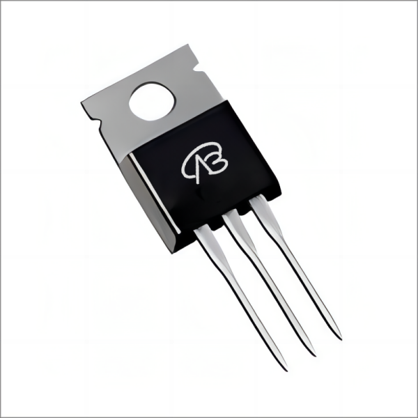
This is a 620V N-channel MOSFET from ST, utilizing the robust TO-220 package. It is part of the MDmesh K3 series, which features an optimized vertical structure delivering very low on-resistance, excellent dynamic performance, and high avalanche capability. Its key advantages are: a drain-source voltage (Vdss) of 620V, a continuous drain current (Id) of 8.4A, and an on-resistance (RDS(on)) of 750mΩ at 10V gate drive. This combination makes it suitable for demanding high-voltage, medium-current switching applications.
Compatibility and Differences of the Domestic Alternative (VBM165R12):
VBsemi's VBM165R12 is also offered in a TO-220 package and serves as a pin-to-pin compatible alternative. The primary differences lie in the electrical parameters: VBM165R12 has a slightly lower voltage rating (650V vs. 620V, which is generally acceptable and often considered equivalent in many designs) and a slightly higher on-resistance of 800mΩ @10V. However, it offers a higher continuous current rating of 12A compared to the original's 8.4A.
Key Application Areas:
Original Model STP10N62K3: Its 620V rating and balanced 8.4A current capability make it ideal for offline switch-mode power supplies (SMPS), power factor correction (PFC) stages, lighting ballasts, and motor drives in the several-hundred-watt range where robustness and proven performance are key.
Alternative Model VBM165R12: With its higher current rating (12A) and comparable voltage rating, it is well-suited for applications requiring a current margin or where designs are being upgraded for higher output power. Its slightly higher RDS(on) may lead to marginally higher conduction losses but can be an excellent cost-effective and available alternative in many 650V-system designs.
Comparative Analysis: STD3N62K3 (DPAK, N-channel) vs. VBE165R04
This comparison focuses on a compact, surface-mount high-voltage MOSFET. The design pursuit for the original STD3N62K3 is to bring the benefits of the MDmesh K3 technology—low resistance, fast switching, and avalanche ruggedness—into a space-saving DPAK package.
Analysis of the Original Model (STD3N62K3) Core:
This 620V N-channel MOSFET in a DPAK package is engineered for high-density power boards. Its core advantages are:
High Voltage in Compact Form: Delivers 620V breakdown voltage in a surface-mount package.
Optimized for Switching: The MDmesh K3 technology ensures low gate charge and good dynamic performance for efficient high-frequency switching.
Application-Tailored: With a continuous current of 2.7A and an on-resistance of 2.5Ω @10V, it targets lower-power but high-voltage switching nodes.
Compatibility and Differences of the Domestic Alternative (VBE165R04):
VBsemi's VBE165R04 comes in a TO-252 (DPAK) package, offering direct footprint compatibility. It presents a mixed parameter profile: a higher voltage rating of 650V and a higher continuous current rating of 4A. However, its on-resistance is significantly higher, specified at 2200mΩ @10V (2.2Ω) and 2750mΩ @4.5V.
Key Application Areas:
Original Model STD3N62K3: Its combination of 620V rating, 2.7A current, and 2.5Ω on-resistance makes it a precise fit for auxiliary power supplies, offline converters for low-power appliances, snubber circuits, and as a switch in high-voltage LED drivers where package size is constrained.
Alternative Model VBE165R04: With its higher current (4A) and voltage (650V) ratings, it can be considered for applications where the primary requirement is voltage withstand and a higher current safety margin, and where the higher conduction loss (due to higher RDS(on)) is acceptable or can be managed thermally. It serves as a viable alternative in scenarios prioritizing availability and cost over minimal conduction loss.
Conclusion
In summary, this analysis reveals two distinct substitution strategies for high-voltage applications:
For the TO-220 package N-channel applications, the original STP10N62K3 offers a proven 620V / 8.4A / 750mΩ balance for medium-power offline converters. Its domestic alternative VBM165R12 provides a compatible package with a higher current rating (12A) at a slightly higher on-resistance (800mΩ), making it a strong candidate for designs needing more current headroom or facing supply chain constraints.
For the DPAK package N-channel applications focused on compact high-voltage switching, the original STD3N62K3 (620V / 2.7A / 2.5Ω) is optimized for efficient operation in space-constrained auxiliary power and lighting circuits. The domestic alternative VBE165R04 shifts the balance, offering higher voltage (650V) and current (4A) ratings but with substantially higher on-resistance (~2.2Ω), positioning it as a suitable alternative where voltage/current margin is critical and the associated conduction loss is permissible.
The core takeaway is that selection is driven by precise application requirements. In the current landscape, domestic alternatives like VBM165R12 and VBE165R04 not only provide reliable backup options but also offer different performance trade-offs (e.g., higher current vs. higher RDS(on)), granting engineers greater flexibility in design optimization, cost control, and supply chain resilience. A deep understanding of each device's parameter implications is essential to leverage its full value within the circuit.


 Download now
 中文
中文 English
 Back to previous page


