MOSFET Selection for High-Voltage Power Applications: STF7NM60N, STD6N65M2 vs. China Alternatives VBMB165R10, VBE165R05S
MOSFET Selection for High-Voltage Power Applications: STF7NM60N, STD6N65M2 vs. China Alternatives VBMB165R10, VBE165R05S
In high-voltage power conversion and switching applications, selecting a MOSFET that balances voltage rating, conduction loss, and switching performance is a critical task for engineers. This involves careful trade-offs among efficiency, reliability, cost, and supply chain diversity. This article takes two representative high-voltage MOSFETs, STF7NM60N (N-channel) and STD6N65M2 (N-channel), as benchmarks. It deeply analyzes their design cores and application scenarios, while comparatively evaluating two domestic alternative solutions, VBMB165R10 and VBE165R05S. By clarifying parameter differences and performance orientations, we aim to provide a clear selection guide to help you find the most suitable power switching solution in the complex component landscape.
Comparative Analysis: STF7NM60N (N-channel) vs. VBMB165R10
Analysis of the Original Model (STF7NM60N) Core:
This is a 600V N-channel MOSFET from STMicroelectronics, utilizing a TO-220FP package. Its design core is based on the second-generation MDmesh technology, combining a vertical structure with a strip layout to achieve an excellent balance of low on-resistance and low gate charge. Key advantages include: a drain-source voltage (Vdss) of 600V, a continuous drain current (Id) of 5A, and a typical on-resistance (RDS(on)) of 900mΩ at 10V gate drive. This makes it highly suitable for demanding high-efficiency converters.
Compatibility and Differences of the Domestic Alternative (VBMB165R10):
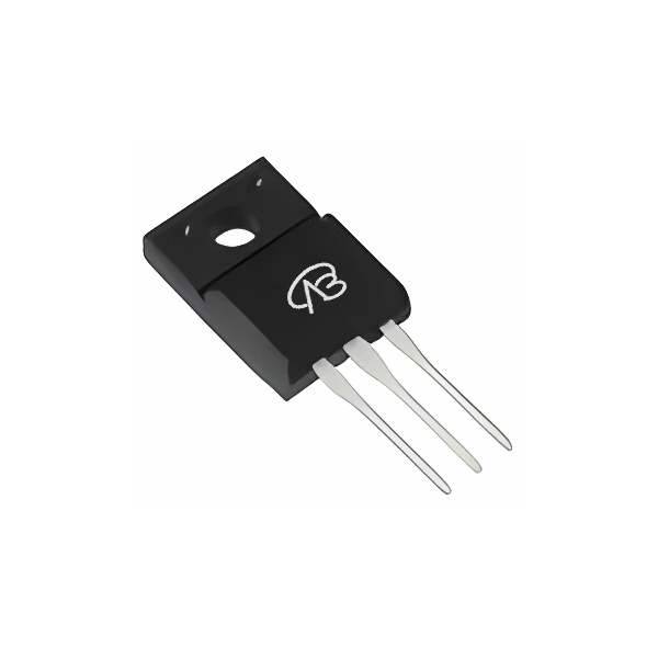
VBsemi's VBMB165R10 is offered in a TO-220F package and serves as a functional alternative. The main differences lie in the electrical parameters: VBMB165R10 features a higher voltage rating (650V) and a slightly lower on-resistance of 830mΩ at 10V. However, its continuous drain current is rated higher at 10A. It utilizes a planar technology, differing from the MDmesh structure of the original.
Key Application Areas:
Original Model STF7NM60N: Its characteristics make it well-suited for high-voltage, medium-power switching applications requiring good efficiency. Typical applications include:
Switch-Mode Power Supplies (SMPS): Such as flyback or forward converters in AC-DC power adapters and auxiliary power supplies.
Power Factor Correction (PFC) stages: In boost PFC circuits for industrial and consumer electronics.
Lighting ballasts and motor drives: For controlling inductive loads.
Alternative Model VBMB165R10: With its higher voltage and current ratings, it is suitable for applications requiring greater voltage margin and higher current capability, potentially offering an upgrade path in similar SMPS and PFC circuits where lower conduction loss is desired.
Comparative Analysis: STD6N65M2 (N-channel) vs. VBE165R05S
This comparison focuses on high-voltage MOSFETs in surface-mount packages, where the balance between voltage withstand, on-resistance, and thermal performance in a compact footprint is key.
Analysis of the Original Model (STD6N65M2) Core:
This is a 650V N-channel MOSFET from STMicroelectronics in a DPAK package. It leverages the MDmesh M2 technology, aiming for low on-resistance in a cost-effective power package. Its core advantages are: a high drain-source voltage of 650V, a continuous drain current of 4A, and a typical on-resistance of 1.35Ω at 10V gate drive. The DPAK package offers a good compromise between power handling and board space.
Compatibility and Differences of the Domestic Alternative (VBE165R05S):
VBsemi's VBE165R05S comes in a TO-252 (DPAK compatible) package, offering direct pin-to-pin compatibility. The key differences are in parameters: It shares the same 650V voltage rating but offers a higher continuous drain current of 5A. Its on-resistance is specified at 1000mΩ (1.0Ω) at 10V, which is lower than the original's 1.35Ω. It employs a Super Junction Multi-EPI technology.
Key Application Areas:
Original Model STD6N65M2: Its combination of 650V rating and DPAK package makes it a reliable choice for space-constrained, medium-power offline applications. For example:
Compact AC-DC power supplies: Primary-side switches in flyback converters for adapters, chargers, and appliances.
LED driver circuits: Providing efficient switching for constant-current LED drivers.
Industrial control auxiliary power.
Alternative Model VBE165R05S: With its lower on-resistance and higher current rating, it presents a performance-enhanced alternative for similar applications, potentially offering improved efficiency and thermal performance in DPAK-based designs for SMPS and LED lighting.
In summary, this comparative analysis reveals two distinct selection paths:
For 600V-650V medium-power applications in through-hole designs, the original model STF7NM60N, with its MDmesh technology offering 900mΩ on-resistance and 5A current in a TO-220FP package, remains a strong candidate for efficient SMPS and PFC stages. Its domestic alternative VBMB165R10 provides a viable option with higher voltage (650V) and current (10A) ratings and slightly lower on-resistance, suitable for designs seeking enhanced margins or an alternative source.
For 650V applications in surface-mount (DPAK) designs, the original model STD6N65M2, with its 1.35Ω on-resistance and 4A capability, is a established choice for compact offline power supplies. The domestic alternative VBE165R05S offers a pin-compatible, performance-competitive solution with lower on-resistance (1.0Ω) and higher current (5A), making it an attractive upgrade or alternative for efficiency-focused DPAK designs.
The core conclusion is: Selection is not about absolute superiority but precise requirement matching. In the context of supply chain diversification, domestic alternatives not only provide feasible backup options but also offer performance parity or even advantages in specific parameters, giving engineers more flexible and resilient choices in design trade-offs and cost control. Understanding the design philosophy and parameter implications of each device is essential to maximize its value in the circuit.


 Download now