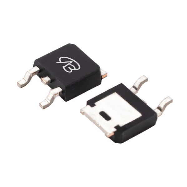
MOSFET Selection for High-Power & High-Voltage Applications: STD52P3LLH6, STB11NK50ZT4 vs. China Alternatives VBE2311, VBL15R10S
MOSFET Selection for High-Power & High-Voltage Applications: STD52P3LLH6, STB11NK50ZT4 vs. China Alternatives VBE2311, VBL15R10S
In high-power and high-voltage circuit designs, selecting a MOSFET that balances robust performance, thermal management, and cost is a critical task for engineers. This goes beyond simple part substitution—it requires careful consideration of electrical characteristics, package capabilities, and supply chain stability. This article takes two representative MOSFETs from STMicroelectronics—STD52P3LLH6 (P-channel) and STB11NK50ZT4 (N-channel)—as benchmarks. We will deeply analyze their design cores and application scenarios, and provide a comparative evaluation of two domestic alternative solutions: VBE2311 and VBL15R10S. By clarifying parameter differences and performance orientations, we aim to offer a clear selection guide to help you identify the most suitable power switching solution in the complex component landscape.
Comparative Analysis: STD52P3LLH6 (P-channel) vs. VBE2311
Analysis of the Original Model (STD52P3LLH6) Core:
This is a 30V P-channel MOSFET from STMicroelectronics, housed in a DPAK package. Its design core focuses on delivering high-current handling in a robust, industry-standard package. Key advantages include an exceptionally high continuous drain current rating of 52A and a low on-resistance of 17mΩ at a 4.5V gate drive. This combination makes it ideal for applications requiring minimal conduction loss under high load currents.
Compatibility and Differences of the Domestic Alternative (VBE2311):
VBsemi's VBE2311, offered in a TO-252 package (similar footprint to DPAK), serves as a pin-to-pin compatible alternative. The key differences lie in its electrical parameters: VBE2311 features a slightly higher voltage rating (-30V) and offers improved on-resistance performance—13mΩ at 4.5V and 11mΩ at 10V. However, its continuous current rating (-60A) is notably higher than the original, while its gate threshold voltage is specified at -2.5V.
Key Application Areas:
Original Model STD52P3LLH6: Its high current capability (52A) and low RDS(on) make it perfectly suited for high-side switching in low-voltage, high-current power paths. Typical applications include:
High-current load switches and power distribution in 12V/24V systems.
Battery protection circuits and discharge path management in high-capacity battery packs.
Motor drive control and solenoid drivers in automotive or industrial settings.
Alternative Model VBE2311: With its lower on-resistance and higher current rating, it is an excellent choice for upgrade scenarios demanding even lower conduction losses and higher power density in similar 30V P-channel applications, such as enhanced power management modules or more efficient motor drives.
Comparative Analysis: STB11NK50ZT4 (N-channel) vs. VBL15R10S
This comparison shifts to high-voltage switching, where the design pursuit balances breakdown voltage, switching performance, and ruggedness.
Analysis of the Original Model (STB11NK50ZT4) Core:
Part of ST's SuperMESH series, this 500V N-channel MOSFET in a D2PAK package is optimized for high-voltage, medium-power applications. Its core advantages are:
High Voltage Robustness: A 500V drain-source voltage rating ensures reliability in off-line or high-voltage bus applications.
Optimized Technology: The SuperMESH technology minimizes on-resistance (520mΩ at 10V) while ensuring excellent dynamic dv/dt capability for demanding switching environments.
Package for Power: The D2PAK package provides superior thermal performance for its 10A continuous current rating.
Compatibility and Differences of the Domestic Alternative (VBL15R10S):
VBsemi's VBL15R10S, in a TO-263 package (compatible with D2PAK), presents a "performance-enhanced" alternative. It matches the 500V voltage rating but offers significantly better conduction characteristics: a much lower on-resistance of 380mΩ at 10V while maintaining the same 10A continuous current rating. This is achieved using a SJ_Multi-EPI (Super Junction Multi-Epitaxial) process.
Key Application Areas:
Original Model STB11NK50ZT4: Its high voltage rating and robust SuperMESH design make it ideal for harsh, high-voltage switching environments. Typical applications include:
Switched-Mode Power Supplies (SMPS) for industrial and consumer electronics.
Power Factor Correction (PFC) stages.
Lighting ballasts and inverter circuits.
Alternative Model VBL15R10S: With its substantially lower on-resistance (380mΩ vs. 520mΩ), it is better suited for applications where higher efficiency and reduced conduction losses are critical within the same 500V/10A range, such as in next-generation, higher-efficiency SMPS designs or compact inverter modules.
Conclusion
In summary, this analysis reveals two distinct selection pathways based on voltage and current needs:
For low-voltage (30V), high-current P-channel applications, the original STD52P3LLH6 offers a proven, high-current (52A) solution in a DPAK package. Its domestic alternative, VBE2311, provides a compelling upgrade with lower on-resistance and a higher current rating (-60A), making it an excellent choice for designs prioritizing maximum efficiency and power density in similar voltage domains.
For high-voltage (500V), medium-current N-channel applications, the original STB11NK50ZT4 delivers reliable performance and ruggedness for demanding switching scenarios thanks to its SuperMESH technology. The domestic alternative VBL15R10S achieves a clear "performance enhancement" with its significantly lower on-resistance (380mΩ), enabling higher efficiency and potentially cooler operation in next-generation 500V power supplies and inverters.
The core takeaway is that selection is not about absolute superiority but precise requirement matching. In the context of supply chain diversification, domestic alternatives like VBE2311 and VBL15R10S not only provide viable backup options but also offer parameter advancements in key areas, granting engineers greater flexibility and resilience in design trade-offs and cost optimization. Understanding the design philosophy and parameter implications of each device is essential to unlocking its full potential in your circuit.


 Download now