MOSFET Selection for High-Voltage Power Applications: STD16N50M2, STP10N60M2 vs. China Alternatives VBE15R15S, VBM165R12
In high-voltage power conversion and switching designs, selecting a MOSFET that balances voltage rating, conduction loss, and ruggedness is a critical engineering challenge. This involves careful trade-offs among performance, cost, thermal management, and supply chain security. This article uses two established high-voltage MOSFETs from STMicroelectronics—STD16N50M2 (500V) and STP10N60M2 (650V)—as benchmarks. We will analyze their design cores, application contexts, and comparatively evaluate two domestic alternative solutions from VBsemi: VBE15R15S and VBM165R12. By clarifying their parameter differences and performance orientations, we aim to provide a clear selection guide for your next high-voltage design.
Comparative Analysis: STD16N50M2 (500V N-Channel) vs. VBE15R15S
Analysis of the Original Model (STD16N50M2) Core:
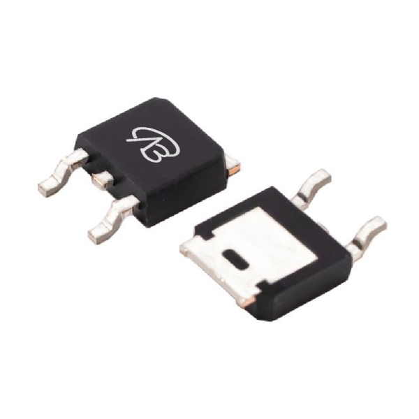
This is a 500V N-channel MOSFET from STMicroelectronics, utilizing the MDmesh M2 technology and packaged in TO-252 (DPAK). Its design core is to offer a robust balance of high voltage capability and switching performance in a compact, surface-mount package. Key advantages include: a rated continuous drain current (Id) of 13A, a typical on-resistance (RDS(on)) of 240mΩ at 10V gate drive, and a high power dissipation (Pd) rating of 110W. This combination makes it suitable for demanding off-line applications.
Compatibility and Differences of the Domestic Alternative (VBE15R15S):
VBsemi's VBE15R15S is also a 500V N-channel MOSFET in a TO-252 package, offering a pin-to-pin compatible alternative. The key differences are in the electrical parameters: VBE15R15S offers a slightly higher continuous current rating of 15A but has a higher typical on-resistance of 290mΩ (@10V) compared to the original's 240mΩ. It utilizes a Super Junction Multi-EPI process.
Key Application Areas:
Original Model STD16N50M2: Its 500V rating and 13A/240mΩ performance make it well-suited for medium-power off-line switch-mode power supplies (SMPS), power factor correction (PFC) stages, and lighting ballasts where efficiency and compact footprint are important.
Alternative Model VBE15R15S: This alternative is suitable for similar 500V application scenarios where a higher current margin (15A) is beneficial, and a slight increase in conduction loss (due to higher RDS(on)) is acceptable or can be managed thermally. It serves as a viable backup or cost-optimized option.
Comparative Analysis: STP10N60M2 (650V N-Channel) vs. VBM165R12
This comparison shifts to higher voltage applications, where the design pursuit is high voltage withstand capability combined with effective switching performance.
Analysis of the Original Model (STP10N60M2) Core:
This 650V N-channel MOSFET from ST, also using MDmesh M2 technology, comes in a through-hole TO-220 package. Its core advantages are:
High Voltage Rating: A 650V drain-source voltage (Vdss) makes it suitable for 85-265VAC off-line applications.
Balanced Performance: It offers a continuous current of 7.5A with a typical on-resistance of 550mΩ (@10V).
Robust Package: The TO-220 package provides excellent thermal dissipation capability for its power level.
Compatibility and Differences of the Domestic Alternative (VBM165R12):
VBsemi's VBM165R12 is a direct package-compatible (TO-220) alternative for 650V applications. It presents a significant "performance-enhanced" profile in key parameters: it boasts a much higher continuous current rating of 12A compared to the original's 7.5A. However, this comes with a higher typical on-resistance of 800mΩ (@10V). It uses a planar technology.
Key Application Areas:
Original Model STP10N60M2: Its 650V/7.5A rating is a classic choice for lower to medium-power off-line SMPS, auxiliary power supplies, and motor drives requiring high voltage blocking.
Alternative Model VBM165R12: This model is more suitable for 650V applications where higher continuous current capability (12A) is the primary requirement, providing significant headroom, and where the higher conduction loss (from 800mΩ RDS(on)) can be accommodated through thermal design. It is an option for designs needing current capability upgrades.
Summary and Selection Paths:
This analysis reveals two distinct selection scenarios for high-voltage applications:
1. For 500V applications seeking a compact surface-mount solution, the original STD16N50M2 offers a proven balance of 13A current and 240mΩ RDS(on). Its domestic alternative VBE15R15S provides package compatibility with a higher 15A current rating but a moderately higher on-resistance, suitable for cost-sensitive or supply-chain-diversified designs where current margin is prioritized.
2. For 650V applications requiring a through-hole package, the original STP10N60M2 provides reliable 7.5A capability with 550mΩ RDS(on). The domestic alternative VBM165R12 offers a substantial upgrade in current handling to 12A, albeit with increased on-resistance, making it a candidate for designs demanding higher current throughput from a 650V switch.
Core Conclusion: The choice is not about absolute superiority but precise requirement matching. In the context of supply chain diversification, domestic alternatives like VBE15R15S and VBM165R12 provide not only feasible backup options but also parameter-specific advantages (higher current ratings). They offer engineers greater flexibility and resilience in design trade-offs and cost control. Understanding the specific performance trade-offs (current vs. RDS(on)) of each device is essential to leverage its full value in the target circuit.


 Download now
 中文
中文 English
 Back to previous page


