MOSFET Selection for High-Voltage Power Applications: NVB125N65S3, FDA18N50 vs. China Alternatives VBL165R20S, VBPB16R20S
In high-voltage power conversion and switching applications, selecting a MOSFET that balances performance, ruggedness, and cost is a critical engineering decision. This is not merely a component substitution but a strategic evaluation of voltage rating, conduction losses, switching efficiency, and supply chain stability. This article uses two established high-voltage MOSFETs, NVB125N65S3 (650V) and FDA18N50 (500V), as benchmarks. We will delve into their design cores, analyze their key application scenarios, and provide a comparative evaluation of two domestic alternative solutions, VBL165R20S and VBPB16R20S. By clarifying parameter differences and performance orientations, this analysis aims to offer a clear selection guide for your next high-voltage design.
Comparative Analysis: NVB125N65S3 (650V Super-Junction) vs. VBL165R20S
Analysis of the Original Model (NVB125N65S3) Core:
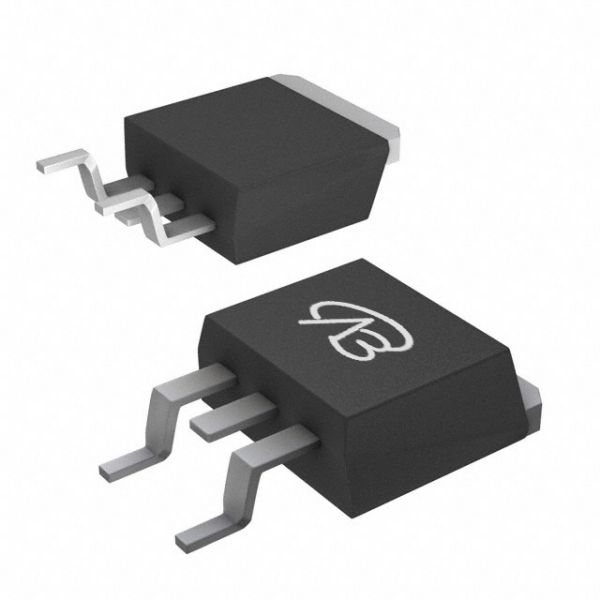
This is a 650V N-channel Super-Junction (SJ) MOSFET from onsemi, in a D2PAK-3 (TO-263-3) package. As part of the SUPERFET III series utilizing charge balance technology, its design core focuses on minimizing conduction and switching losses simultaneously. Key advantages are: a low on-resistance of 125mΩ at a 10V gate drive, supporting a continuous drain current of 24A. The technology delivers excellent switching performance, high dv/dt ruggedness, and aids in simplifying EMI design, making it highly suitable for efficient high-frequency switching.
Compatibility and Differences of the Domestic Alternative (VBL165R20S):
VBsemi's VBL165R20S is also a 650V N-channel SJ MOSFET in a TO-263 package, offering a direct pin-to-pin compatible alternative. The main differences in electrical parameters are: a comparable voltage rating (650V), a slightly higher on-resistance of 160mΩ (@10V), and a slightly lower continuous current rating of 20A compared to the original's 24A. It is based on a similar SJ_Multi-EPI technology platform.
Key Application Areas:
Original Model NVB125N65S3: Its combination of 650V rating, low RDS(on), and superior switching performance makes it ideal for high-efficiency, high-power-density SMPS designs. Typical applications include:
Server/Telecom/Industrial Switch-Mode Power Supplies (SMPS)
Power Factor Correction (PFC) stages
High-voltage DC-DC converters (e.g., for renewable energy, EV charging)
Alternative Model VBL165R20S: A viable domestic alternative for 650V applications where the full 24A current of the original is not required. It suits similar SMPS, PFC, and inverter applications, offering a cost-effective and supply-chain-resilient option with slightly derated current performance.
Comparative Analysis: FDA18N50 (500V Planar MOSFET) vs. VBPB16R20S
Analysis of the Original Model (FDA18N50) Core:
This is a 500V N-channel planar stripe MOSFET from onsemi, in a TO-3PN package. Based on UniFET technology, its design pursues a robust balance of low conduction resistance, good switching performance, and high avalanche energy capability. Its key parameters are: a 500V drain-source voltage, 19A continuous current, and an on-resistance of 265mΩ (@10V, 9.5A). It is engineered for reliability in demanding switching environments.
Compatibility and Differences of the Domestic Alternative (VBPB16R20S):
VBsemi's VBPB16R20S serves as a performance-enhanced alternative. It uses a TO3P package (mechanically similar to TO-3PN) and shifts to a more advanced 600V SJ_Multi-EPI technology. It offers significant parameter improvements: a higher voltage rating (600V), a higher continuous current (20A), and a substantially lower on-resistance of 190mΩ (@10V). This translates to potentially lower conduction losses and a higher power handling margin.
Key Application Areas:
Original Model FDA18N50: Its ruggedness and 500V rating make it a reliable choice for various line-voltage power conversion applications. Typical uses include:
Power Factor Correction (PFC) circuits
Power supplies for Flat Panel Display (FPD) TVs
ATX power supplies
Electronic lighting ballasts
Alternative Model VBPB16R20S: This model is suitable for upgraded or new designs requiring higher voltage margin (600V), lower conduction loss, and higher current capability. It is an excellent choice for next-generation SMPS, PFC stages, and industrial inverters where improved efficiency and power density are desired.
Conclusion
In summary, this analysis reveals two distinct selection pathways for high-voltage applications:
For 650V Super-Junction applications demanding optimal efficiency and switching performance, the original NVB125N65S3, with its low 125mΩ RDS(on) and 24A current rating, presents a strong solution for high-end SMPS and PFC. Its domestic alternative VBL165R20S provides a package-compatible, cost-effective option with slightly adjusted parameters (160mΩ, 20A), suitable for designs where full original performance is not critical.
For 500V/600V robust switching applications, the original FDA18N50 offers proven reliability in planar MOSFET technology for PFC and TV power supplies. The domestic alternative VBPB16R20S emerges as a compelling "performance-upgrade" option, leveraging SJ technology to deliver a higher voltage rating (600V), lower RDS(on) (190mΩ), and higher current (20A), enabling more efficient and compact designs.
The core conclusion is that selection hinges on precise requirement matching. In the context of supply chain diversification, domestic alternatives like VBL165R20S and VBPB16R20S not only provide viable backup options but also offer parameter enhancements in key areas, granting engineers greater flexibility in design trade-offs and cost optimization. Understanding the technology and parameter implications of each device is essential to unlocking its full potential in the circuit.


 Download now