MOSFET Selection for Compact Power and High-Voltage Switching: NTZD3155CT2G, FQD1N60CTM vs. China Alternatives VBTA5220N, VBE165R02
In today’s landscape of circuit miniaturization and efficient power management, selecting the right MOSFET for space-constrained or high-voltage applications is a critical engineering challenge. It goes beyond simple part substitution—it requires careful balancing of performance, size, cost, and supply chain reliability. This article takes two representative MOSFETs, the dual-channel NTZD3155CT2G and the high-voltage FQD1N60CTM, as benchmarks. We will analyze their design cores and application scenarios, and compare them with two domestic alternative solutions: VBTA5220N and VBE165R02. By clarifying parameter differences and performance orientations, we aim to provide a clear selection guide to help you find the most suitable power switching solution for your next design.
Comparative Analysis: NTZD3155CT2G (Dual N+P Channel) vs. VBTA5220N
Analysis of the Original Model (NTZD3155CT2G) Core:
This is a dual MOSFET from onsemi, integrating one N-channel and one P-channel in an ultra-compact SOT-563 package (1.6×1.6 mm). Its design core is to provide efficient, space-saving switching for low-voltage, low-current applications. Key advantages include: a low threshold voltage, ESD-protected gates, and an on-resistance (RDS(on)) of 400mΩ @ 4.5V for the N-channel. It supports a continuous drain current of 540mA per channel, making it ideal for miniaturized designs requiring level shifting or dual switching.
Compatibility and Differences of the Domestic Alternative (VBTA5220N):
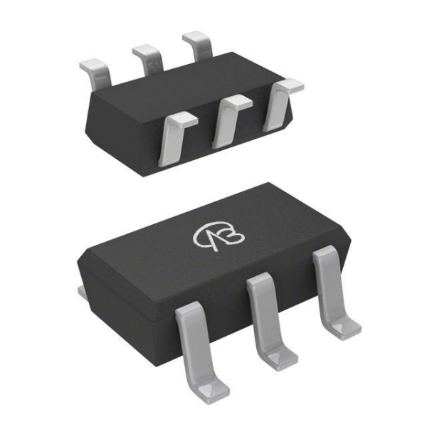
VBsemi’s VBTA5220N is also a dual N+P channel MOSFET in a small SC75-6 package, offering a pin-to-pin compatible alternative. The key differences are in the electrical parameters: VBTA5220N offers a slightly higher gate drive voltage flexibility (±12V vs. the original's implied standard levels) and a significantly lower on-resistance for the N-channel at 4.5V (270mΩ vs. 400mΩ). However, its continuous current rating is slightly lower at 0.6A/-0.3A (N/P) compared to the original's 540mA per channel.
Key Application Areas:
Original Model NTZD3155CT2G: Its ultra-small size and balanced dual-channel performance make it perfect for space-critical, low-power applications.
DC-DC Conversion Circuits: Used in compact power modules for on/off control or synchronous switching.
Load/Power Switching with Level Shifting: Ideal for battery-powered devices, IoT modules, and portable electronics where signal isolation or voltage translation is needed.
Alternative Model VBTA5220N: More suitable for applications requiring slightly better conduction efficiency (lower RDS(on)) at 4.5V drive within a similar current range (<0.6A). It's a strong alternative where package compatibility and improved on-resistance are priorities.
Comparative Analysis: FQD1N60CTM (N-channel) vs. VBE165R02
This comparison shifts focus from miniaturization to high-voltage, medium-power switching capability.
Analysis of the Original Model (FQD1N60CTM) Core:
This 600V N-channel MOSFET from onsemi, in a TO-252 (DPAK) package, is designed for robust high-voltage switching. Its core advantages are:
High Voltage Rating: 600V drain-source voltage withstand capability.
Optimized for Switching: Built with planar stripe DMOS technology for a good balance of on-resistance (11.5Ω max @10V) and switching performance, including high avalanche energy strength.
Proven Reliability: Suitable for demanding power supply applications.
Compatibility and Differences of the Domestic Alternative (VBE165R02):
VBsemi’s VBE165R02 is a "performance-enhanced" alternative in the same TO-252 package. It surpasses the original in key parameters:
Higher Voltage & Current Rating: 650V Vdss and a 2A continuous current, compared to 600V and 1A.
Lower On-Resistance: Significantly lower RDS(on) of 4300mΩ (4.3Ω) @10V versus 11.5Ω, leading to reduced conduction losses and lower operating temperatures.
Key Application Areas:
Original Model FQD1N60CTM: A reliable choice for standard high-voltage, low-to-medium current switching.
Switching Power Supplies (SMPS): Auxiliary power sections or lower-power primary-side switching.
Active Power Factor Correction (PFC): Lower-current stages in PFC circuits.
Electronic Lamp Ballasts: For fluorescent or LED driver circuits.
Alternative Model VBE165R02: Better suited for upgraded designs requiring higher efficiency, higher current capability (up to 2A), and a greater voltage margin. It is ideal for more demanding SMPS, PFC stages, or motor drives where lower loss is critical.
Conclusion
This analysis reveals two distinct selection pathways:
For ultra-compact, low-power dual-channel switching, the original NTZD3155CT2G offers an excellent balance of tiny size and sufficient performance for DC-DC conversion and level shifting. Its domestic alternative, VBTA5220N, provides package compatibility with the advantage of lower on-resistance at 4.5V, making it a compelling choice for efficiency-sensitive designs within its current range.
For high-voltage, medium-power switching, the original FQD1N60CTM is a proven, reliable component for 600V applications like SMPS and ballasts. The domestic alternative VBE165R02 offers a significant performance upgrade with higher voltage (650V), higher current (2A), and much lower on-resistance, enabling higher efficiency and power density in next-generation designs.
The core takeaway is that selection is about precise requirement matching. In an era of supply chain diversification, domestic alternatives like VBTA5220N and VBE165R02 not only provide viable backups but also offer performance enhancements in specific areas, giving engineers greater flexibility and resilience in design trade-offs and cost optimization. Understanding the design philosophy and parameter implications of each device is key to unlocking its full potential in your circuit.


 Download now