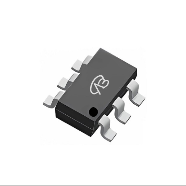
MOSFET Selection for Compact Power Applications: NTJD4105CT1G, NDS0610 vs. China Alternatives VBK5213N, VB264K
In the pursuit of device miniaturization and high efficiency today, selecting a MOSFET that is 'just right' for a compact circuit board is a practical challenge faced by every engineer. This is not merely completing a substitution from a model list, but a precise trade-off among performance, size, cost, and supply chain resilience. This article will use the two highly representative MOSFETs, NTJD4105CT1G (Complementary Dual) and NDS0610 (P-channel), as benchmarks, deeply analyze their design cores and application scenarios, and comparatively evaluate the two domestic alternative solutions, VBK5213N and VB264K. By clarifying the parameter differences and performance orientations among them, we aim to provide you with a clear selection map, helping you find the most matching power switching solution for your next design in the complex world of components.
Comparative Analysis: NTJD4105CT1G (Complementary Dual) vs. VBK5213N
Analysis of the Original Model (NTJD4105CT1G) Core:
This is a 20V Complementary Dual (1 N-Channel + 1 P-Channel) MOSFET from onsemi, using a compact SOT-363 package (2 x 2 mm). Its design core is to achieve minimal footprint and improved circuit efficiency in space-constrained designs. The key advantages are: low on-resistance (RDS(on) of 360mΩ @2.5V for the N-channel) and a continuous drain current of 910mA. This low RDS(on) performance is particularly suitable for single or dual-cell Li-ion battery-powered portable devices.
Compatibility and Differences of the Domestic Alternative (VBK5213N):
VBsemi's VBK5213N also uses a small SC70-6 package and is a dual N+P channel MOSFET. The main differences and advantages lie in the electrical parameters: VBK5213N offers significantly lower on-resistance (RDS(2.5V): 110/190 mΩ for N/P channels respectively) compared to the original, and higher continuous current capability (3.28A/-2.8A for N/P channels).
Key Application Areas:
Original Model NTJD4105CT1G: Its characteristics are very suitable for compact portable devices requiring complementary switching pairs. Typical applications include:
Power management and load switching in smartphones, media players, digital cameras, and PDAs.
Signal routing and power domain isolation in battery-powered IoT devices.
Alternative Model VBK5213N: More suitable for upgraded scenarios demanding lower conduction loss and higher current capability in a similar tiny footprint, making it an excellent performance-enhanced drop-in replacement for efficiency-critical portable applications.
Comparative Analysis: NDS0610 (P-channel) vs. VB264K
Unlike the complementary dual model focusing on minimal footprint, the design pursuit of this P-channel MOSFET is 'high-voltage switching with low current'.
Analysis of the Original Model (NDS0610) Core:
The core advantages of the original model are reflected in:
High Voltage Rating: A drain-source voltage (Vdss) of -60V, suitable for off-line or higher voltage side switching.
Low Current Switching: Designed for applications requiring up to 120mA continuous current, capable of handling up to 1A pulses.
Proven Technology: Manufactured using high cell-density DMOS technology for robust performance and fast switching.
Compatibility and Differences of the Domestic Alternative (VB264K):
The domestic alternative VB264K is a direct SOT23-3 package compatible part. It matches the high voltage rating (-60V) and is optimized for similar low-current, high-side switching applications. Its key parameters include an on-resistance of 3000mΩ @10V and a continuous drain current of -0.5A.
Key Application Areas:
Original Model NDS0610: Its high voltage and low current characteristics make it ideal for specific niche applications. For example:
Low-current high-side switches in low-voltage systems.
Signal isolation or auxiliary power switching in consumer electronics.
Alternative Model VB264K: Serves as a reliable domestic alternative for applications requiring a 60V P-channel MOSFET in a SOT-23 package, suitable for similar high-side switching, load management, or signal control circuits where the original part is specified.
Conclusion
In summary, this comparative analysis reveals two clear selection paths:
For complementary dual MOSFET applications in ultra-compact portable devices, the original model NTJD4105CT1G, with its integrated N+P pair in a 2x2mm package, is a classic choice for space-constrained battery-powered designs. Its domestic alternative VBK5213N provides a significant "performance-enhanced" option, offering substantially lower on-resistance and higher current capability in a similarly small SC70-6 package, making it an excellent upgrade for improving efficiency.
For specific low-current, high-voltage P-channel switching needs, the original NDS0610 serves its purpose in niche applications. The domestic alternative VB264K provides a direct package-compatible and parameter-equivalent replacement, ensuring supply chain flexibility for this specific part type.
The core conclusion is: There is no absolute superiority or inferiority in selection; the key lies in precise matching of requirements. In the context of supply chain diversification, domestic alternative models not only provide feasible backup options but also achieve surpassing in specific parameters (as seen with VBK5213N), offering engineers more flexible and resilient choice space in design trade-offs and cost control. Understanding the design philosophy and parameter implications of each device is essential to maximize its value in the circuit.


 Download now