MOSFET Selection for Power Switching and Signal Control: NTB25P06T4G, FDG6301N vs. China Alternatives VBL2658, VBK3215N
In the design of power electronics and compact signal control circuits, selecting the appropriate MOSFET is crucial for achieving reliability, efficiency, and cost-effectiveness. This article takes two representative MOSFETs from onsemi—the power-focused NTB25P06T4G (P-channel) and the signal-level FDG6301N (dual N-channel)—as benchmarks. It deeply analyzes their design cores and application scenarios, while providing a comparative evaluation of two domestic alternative solutions: VBL2658 and VBK3215N. By clarifying parameter differences and performance orientations, this article aims to offer a clear selection guide to help you find the most suitable switching solution in the complex component landscape.
Comparative Analysis: NTB25P06T4G (P-channel) vs. VBL2658
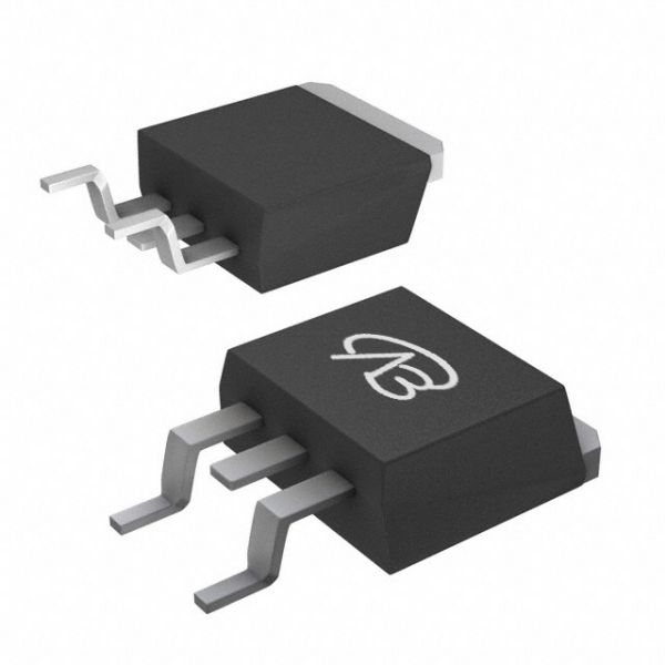
Analysis of the Original Model (NTB25P06T4G) Core:
This is a 60V P-channel MOSFET from onsemi in a D2PAK package. Its design core is to provide robust, high-energy switching capability for power applications. Key advantages include: a drain-source voltage (Vdss) of 60V, a continuous drain current (Id) of 27.5A, and an on-resistance (RDS(on)) of 82mΩ at 10V gate drive. It is specifically engineered to withstand high energy in avalanche and commutation modes, offering an additional safety margin against unexpected voltage transients.
Compatibility and Differences of the Domestic Alternative (VBL2658):
VBsemi's VBL2658 is a P-channel MOSFET in a TO-263 package, serving as a functional alternative for power switching. The main differences are in electrical parameters: VBL2658 has a similar voltage rating (-60V) but offers a higher continuous current (-35A) and a significantly lower on-resistance (48mΩ @10V) compared to the original.
Key Application Areas:
Original Model NTB25P06T4G: Ideal for low-voltage, high-speed switching applications where ruggedness and commutation safe operating area are critical. Typical uses include:
Bridge circuits in power supplies, converters, and motor control.
Applications requiring diode speed and safety against voltage transients.
Alternative Model VBL2658: More suitable for power switching applications demanding higher current capability (up to -35A) and lower conduction loss (48mΩ), such as upgraded power modules, motor drives, or DC-DC converters where efficiency and thermal performance are prioritized.
Comparative Analysis: FDG6301N (Dual N-channel) vs. VBK3215N
Analysis of the Original Model (FDG6301N) Core:
This is a dual N-channel logic-level enhancement-mode MOSFET from onsemi in an ultra-compact SC-70-6 package. Its design pursuit is to minimize on-resistance for low-voltage signal switching. Core advantages include: a drain-source voltage (Vdss) of 25V per channel, a continuous drain current (Id) of 220mA per channel, and an on-resistance of 4Ω at 4.5V gate drive. It is produced using a proprietary high-cell-density DMOS process, making it suitable for replacing bipolar digital transistors and small-signal MOSFETs in low-voltage applications.
Compatibility and Differences of the Domestic Alternative (VBK3215N):
VBsemi's VBK3215N is a dual N-channel MOSFET in an SC70-6 package, offering direct pin-to-pin compatibility. It provides significant performance enhancement: while the voltage rating is slightly lower (20V), it boasts a much higher continuous current (2.6A total) and dramatically lower on-resistance (86mΩ @4.5V per channel).
Key Application Areas:
Original Model FDG6301N: Perfect for space-constrained, low-voltage signal-level switching and amplification. Typical applications include:
Replacement for bipolar digital transistors and small-signal MOSFETs.
Load switching in portable devices, IoT sensors, and low-power modules.
Signal routing and interface control in consumer electronics.
Alternative Model VBK3215N: Excellent for applications requiring higher current handling and much lower conduction loss in a compact dual N-channel footprint. Ideal for:
Enhanced load switches and power management in compact devices.
Signal conditioning circuits where lower voltage drop is critical.
Upgrading existing designs for better efficiency and current capacity.
Conclusion
This analysis reveals two distinct selection paths:
For rugged power switching in applications like motor control and bridge circuits, the original NTB25P06T4G offers proven reliability with its 60V/27.5A rating and avalanche ruggedness. Its domestic alternative VBL2658 provides a compelling upgrade with higher current (-35A) and lower on-resistance (48mΩ), making it suitable for designs prioritizing efficiency and power density.
For compact signal-level switching, the original FDG6301N is a proven solution for low-current (220mA), low-voltage signal replacement. Its domestic alternative VBK3215N delivers a substantial performance boost with much higher current (2.6A) and drastically lower on-resistance (86mΩ), enabling more robust signal switching and power management in the same tiny SC70-6 footprint.
The core takeaway is that selection depends on precise requirement matching. Domestic alternatives not only provide supply chain resilience but also offer opportunities for performance enhancement and cost optimization in specific applications. Understanding each device's design intent and parameter implications is key to maximizing its value in your circuit.


 Download now
 中文
中文 English
 Back to previous page


