MOSFET Selection for High-Power and Integrated Switch Applications: HUF75645S3ST, FDC6321C vs. China Alternatives VBL1101N, VB5222
In modern power design, balancing high-current handling, integration, and cost-effectiveness is a critical challenge. This article takes two representative MOSFETs from onsemi—the high-power HUF75645S3ST (N-channel) and the integrated dual-channel FDC6321C—as benchmarks. It deeply analyzes their design cores and application scenarios, while providing a comparative evaluation of their domestic alternatives, VBL1101N and VB5222. By clarifying parameter differences and performance orientations, we aim to offer a clear selection guide for your next power switching solution.
Comparative Analysis: HUF75645S3ST (N-channel) vs. VBL1101N
Analysis of the Original Model (HUF75645S3ST) Core:
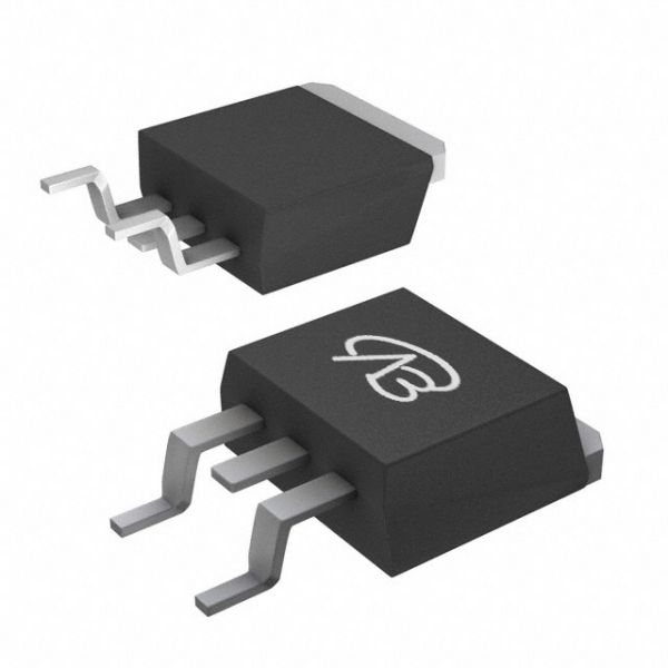
This is a 100V, 75A N-channel UltraFET Power MOSFET from onsemi in a D2PAK package. Its design core is to deliver robust power handling and efficient conduction in high-current applications. Key advantages include a low on-resistance of 14mΩ (at 10V, 75A) and a high continuous drain current rating of 75A, making it suitable for demanding circuits where minimizing conduction loss is paramount.
Compatibility and Differences of the Domestic Alternative (VBL1101N):
VBsemi's VBL1101N is also a 100V N-channel MOSFET in a TO-263 package, offering a viable alternative. The key differences are in the electrical parameters: VBL1101N boasts a lower on-resistance of 10mΩ (at 10V) and a higher continuous current rating of 100A, indicating superior conduction performance. However, designers must verify pin compatibility and thermal performance for their specific layout.
Key Application Areas:
Original Model HUF75645S3ST: Ideal for high-power applications requiring reliable 100V switching and high current capacity. Typical uses include:
Motor drives for industrial equipment or electric vehicles.
High-current DC-DC converters and power supplies.
Inverter and UPS systems.
Alternative Model VBL1101N: Suited for upgrade scenarios demanding even lower conduction loss (10mΩ RDS(on)) and higher current handling (100A) within the same voltage class, potentially offering efficiency gains in similar high-power circuits.
Comparative Analysis: FDC6321C (Dual N+P Channel) vs. VB5222
Analysis of the Original Model (FDC6321C) Core:
This onsemi device is a dual N and P-channel logic-level MOSFET in a compact TSOT-23-6 package. Its design core is high-density DMOS technology to minimize on-resistance for low-voltage load switching. It integrates both channel types, simplifying design by replacing digital transistors and their bias resistors. Key parameters include a drain-source voltage of 25V and on-resistance as low as 450mΩ (for one channel at 4.5V).
Compatibility and Differences of the Domestic Alternative (VB5222):
VBsemi's VB5222 is a direct functional alternative—a dual N+P channel MOSFET in an SOT23-6 package. It offers enhanced performance in key areas: a higher voltage rating of ±20V and significantly lower on-resistance (e.g., 22mΩ for N-channel, 55mΩ for P-channel at 10V). Its current rating (5.5A/3.4A) is also substantially higher than the FDC6321C's.
Key Application Areas:
Original Model FDC6321C: Perfect for space-constrained, low-voltage load switching and signal routing where integration simplifies the BOM. Typical applications include:
Power management in portable devices (phones, tablets).
Load switches for peripherals and modules.
Signal line switching and level translation.
Alternative Model VB5222: An excellent "performance-enhanced" replacement, better suited for applications requiring higher voltage tolerance (±20V), lower conduction losses, and higher load current capability, while maintaining the integration benefits of a dual-channel device.
Conclusion
This analysis reveals two distinct upgrade paths:
1. For high-power, high-current applications, the original HUF75645S3ST offers a solid 75A, 14mΩ solution. Its domestic alternative VBL1101N presents a compelling performance upgrade with 100A current and 10mΩ RDS(on), ideal for designs pushing efficiency and power density limits in motor drives and converters.
2. For compact, integrated load switching, the FDC6321C provides essential dual-channel functionality. The domestic alternative VB5222 significantly outperforms it in voltage rating, on-resistance, and current capacity, making it a superior choice for more demanding low-voltage switch applications without sacrificing board space.
The core takeaway is that selection hinges on precise requirement matching. In the context of supply chain diversification, domestic alternatives like VBL1101N and VB5222 not only provide reliable backup options but also offer tangible performance enhancements, giving engineers greater flexibility in design trade-offs and cost optimization. Understanding each device's design philosophy and parameter implications is key to unlocking its full potential in your circuit.


 Download now