MOSFET Selection for High-Voltage and Miniature Applications: FQPF4N90C, NTJD4001NT1G vs. China Alternatives VBMB195R06, VBK3215N
In power design, balancing high-voltage handling, switching efficiency, and space constraints is a critical challenge. This article takes two representative MOSFETs—FQPF4N90C (high-voltage N-channel) and NTJD4001NT1G (dual N-channel miniature switch)—as benchmarks. It analyzes their design cores and application scenarios, while evaluating domestic alternative solutions VBMB195R06 and VBK3215N. By clarifying parameter differences and performance orientations, we provide a clear selection map to help you find the optimal power switching solution.
Comparative Analysis: FQPF4N90C (N-channel) vs. VBMB195R06
Analysis of the Original Model (FQPF4N90C) Core:
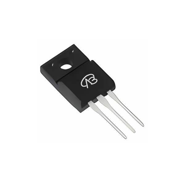
This is a 900V N-channel MOSFET from onsemi, in a TO-220F-3 package. Its design focuses on robust high-voltage switching in a standard isolated package. Key advantages are: a high drain-source voltage (Vdss) of 900V, a continuous drain current (Id) of 4A, and an on-resistance of 4.2Ω at 10V gate drive. It suits applications requiring reliable off-line switching.
Compatibility and Differences of the Domestic Alternative (VBMB195R06):
VBsemi’s VBMB195R06 is a pin-to-pin compatible alternative in a TO220F package. The main differences are electrical: VBMB195R06 offers a higher voltage rating (950V vs. 900V) and a higher continuous current (6A vs. 4A). Crucially, its on-resistance is significantly lower at 2400mΩ (2.4Ω) @ 10V compared to 4.2Ω, promising lower conduction losses.
Key Application Areas:
Original Model FQPF4N90C: Ideal for high-voltage, medium-current switching where cost-effectiveness and proven reliability are key. Typical uses include:
Off-line switch-mode power supplies (SMPS) like flyback converters.
Power factor correction (PFC) stages in low-to-mid power applications.
Electronic ballasts and lighting controls.
Alternative Model VBMB195R06: Better suited for applications demanding higher voltage margin, higher current capability (up to 6A), and lower conduction loss. It’s a performance-enhanced choice for upgraded SMPS, PFC circuits, or industrial controls where efficiency is critical.
Comparative Analysis: NTJD4001NT1G (Dual N-channel) vs. VBK3215N
This comparison shifts to space-constrained, low-voltage signal and power switching. The original model’s design pursues miniaturization and protection features.
Analysis of the Original Model (NTJD4001NT1G) Core:
This onsemi component integrates two 30V N-channel MOSFETs in a tiny SOT-363 package (30% smaller than TSOP-6). Its core advantages are:
Space Saving: Ultra-compact footprint for dense PCB layouts.
Protected & Robust: Gate ESD protection and AEC-Q101 qualification enhance reliability.
Fast Switching: Low gate charge enables quick switching, suitable for load control.
Key Parameters: Vdss=30V, Id=250mA per channel, RDS(on)=2.5Ω @ 2.5V.
Compatibility and Differences of the Domestic Alternative (VBK3215N):
VBsemi’s VBK3215N is a direct pin-to-pin alternative in an SC70-6 package. It represents a major performance upgrade:
Higher Current: 2.6A continuous current per channel vs. 250mA.
Dramatically Lower RDS(on): 110mΩ @ 2.5V and 86mΩ @ 4.5V, compared to 2.5Ω. This drastically reduces conduction loss and voltage drop.
Slightly Lower Voltage Rating: 20V Vdss vs. 30V, sufficient for many low-voltage applications.
Key Application Areas:
Original Model NTJD4001NT1G: Perfect for protected, miniature signal switching and very low-power load control in portable electronics. Typical uses:
Load switches in battery-powered devices (phones, PDAs, cameras).
Signal routing and isolation in communication modules.
General-purpose low-side switching where AEC-Q101 compliance is needed.
Alternative Model VBK3215N: Ideal for applications requiring much higher current handling and minimal loss in a similarly small package. It excels in:
High-efficiency load switches for modern compact devices.
Power management in portable equipment where low RDS(on) extends battery life.
Space-constrained DC-DC converter synchronous rectification or switching.
Conclusion
This analysis reveals two distinct selection paths:
For high-voltage switching, the original FQPF4N90C offers a reliable 900V/4A solution. Its domestic alternative VBMB195R06 provides a compelling upgrade with higher voltage (950V), higher current (6A), and significantly lower on-resistance for improved efficiency.
For miniature dual-channel switching, the original NTJD4001NT1G delivers ultra-compact, protected switching for low-current signals. Its domestic alternative VBK3215N is a powerhouse upgrade, offering over 10x the current capacity (2.6A) and drastically lower RDS(on) for high-efficiency, space-constrained power switching.
The core conclusion is that selection hinges on precise requirement matching. Domestic alternatives not only provide supply chain resilience but also offer significant performance enhancements in key parameters like current and RDS(on), giving engineers greater flexibility in design trade-offs and cost optimization. Understanding each device's design philosophy is key to unlocking its full potential in your circuit.


 Download now
 中文
中文 English
 Back to previous page


