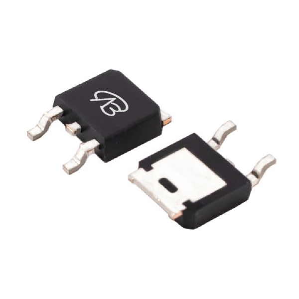
MOSFET Selection for Medium-Voltage Switching and Dual-Channel Applications: FQD10N20CTM, FDS8858CZ vs. China Alternatives VBE1203M, VBA5311
In power supply and battery-powered circuit designs, selecting MOSFETs that balance voltage rating, switching performance, and cost is a critical task for engineers. It’s not just about finding a pin-to-pin replacement, but a careful trade-off among breakdown voltage, conduction loss, switching speed, and supply chain flexibility. This article takes two representative MOSFETs—FQD10N20CTM (200V N‑channel) and FDS8858CZ (30V dual N+P‑channel)—as benchmarks, analyzes their design focus and application scenarios, and evaluates two domestic alternative solutions, VBE1203M and VBA5311. By clarifying parameter differences and performance orientation, we provide a clear selection guide to help you find the most suitable power‑switching solution for your next design.
Comparative Analysis: FQD10N20CTM (200V N‑channel) vs. VBE1203M
Analysis of the Original Model (FQD10N20CTM) Core:
This is a 200V N‑channel MOSFET from onsemi, packaged in TO‑252AA. Its design core is to deliver robust performance in medium‑voltage switching applications. Key advantages include: a drain‑source voltage (Vdss) of 200V, continuous drain current (Id) of 7.8 A, and low gate charge (typically 20 nC) combined with low reverse transfer capacitance (Crss ~40.5 pF). The device is 100% avalanche‑tested and utilizes planar stripe DMOS technology, offering a good balance of low on‑resistance (360 mΩ max. at 10 V VGS) and excellent switching performance, making it suitable for switch‑mode power supplies, active PFC, and electronic lamp ballasts.
Compatibility and Differences of the Domestic Alternative (VBE1203M):
VBsemi’s VBE1203M is also offered in TO‑252 package and serves as a direct pin‑to‑pin alternative. The main differences lie in electrical parameters: VBE1203M features the same 200V voltage rating but offers a higher continuous current (10 A) and a significantly lower on‑resistance (245 mΩ at 10 V VGS) compared to the original’s 360 mΩ. This results in lower conduction loss and improved efficiency in many applications.
Key Application Areas:
Original Model FQD10N20CTM: Well‑suited for 200V‑class switching applications where avalanche ruggedness and reliable switching are priorities, such as:
- Switch‑mode power supplies (SMPS) in AC‑DC converters.
- Active power factor correction (PFC) stages.
- Electronic lighting ballasts.
Alternative Model VBE1203M: With its lower RDS(on) and higher current capability, it is an enhanced drop‑in replacement for the same 200V applications, offering better efficiency and thermal performance in new designs or upgrades.
Comparative Analysis: FDS8858CZ (30V Dual N+P‑channel) vs. VBA5311
Analysis of the Original Model (FDS8858CZ) Core:
This onsemi device integrates an N‑channel and a P‑channel MOSFET in a compact SO‑8 package. It is built using advanced PowerTrench® technology, aiming to minimize on‑resistance while maintaining fast switching. Key parameters include a 30V drain‑source voltage for both channels, continuous drain current of 8.6 A, and a low on‑resistance of 20.5 mΩ (at 10 V VGS for the N‑channel). Its design focuses on low‑power‑loss and high‑speed switching in low‑voltage, battery‑powered applications.
Compatibility and Differences of the Domestic Alternative (VBA5311):
VBsemi’s VBA5311 is also a dual N+P‑channel MOSFET in SOP‑8 package, providing direct pin‑to‑pin compatibility. It offers a higher voltage rating (±30V) and improved conduction performance: the N‑channel RDS(on) is as low as 11 mΩ at 10 V VGS, and the P‑channel RDS(on) is 21 mΩ at 10 V VGS. Continuous current ratings are 10 A (N‑channel) and -8 A (P‑channel), surpassing the original’s current capability.
Key Application Areas:
Original Model FDS8858CZ: Ideal for space‑constrained, low‑voltage applications where both high‑side and low‑side switching are needed, such as:
- Power management in battery‑operated devices.
- Load switches and power‑path control in portable electronics.
- Low‑voltage DC‑DC converters and motor drive circuits.
Alternative Model VBA5311: With its lower on‑resistance and higher current ratings, it is a performance‑enhanced replacement for dual‑channel applications, enabling higher efficiency and greater power‑handling capability in similar circuit topologies.
Conclusion
This comparison reveals two clear selection paths:
For 200V N‑channel switching applications that demand avalanche ruggedness and reliable performance, the original FQD10N20CTM provides a proven solution for SMPS, PFC, and ballast designs. Its domestic alternative VBE1203M offers a pin‑compatible upgrade with lower RDS(on) and higher current capability, making it an attractive option for improved efficiency and thermal behavior.
For low‑voltage dual N+P‑channel applications where space and efficiency are critical, the original FDS8858CZ delivers a compact, balanced solution for battery‑powered and portable systems. The domestic alternative VBA5311 significantly enhances performance with much lower on‑resistance and higher current ratings, providing a superior drop‑in replacement for designs requiring higher power density and lower losses.
The core insight is that selection is not about absolute superiority but about precise requirement matching. In the context of supply‑chain diversification, domestic alternatives like VBE1203M and VBA5311 not only offer reliable backup options but also deliver parameter improvements, giving engineers greater flexibility and resilience in design trade‑offs and cost control. Understanding each device’s design philosophy and parameter implications is essential to maximize its value in your circuit.


 Download now
 中文
中文 English
 Back to previous page


