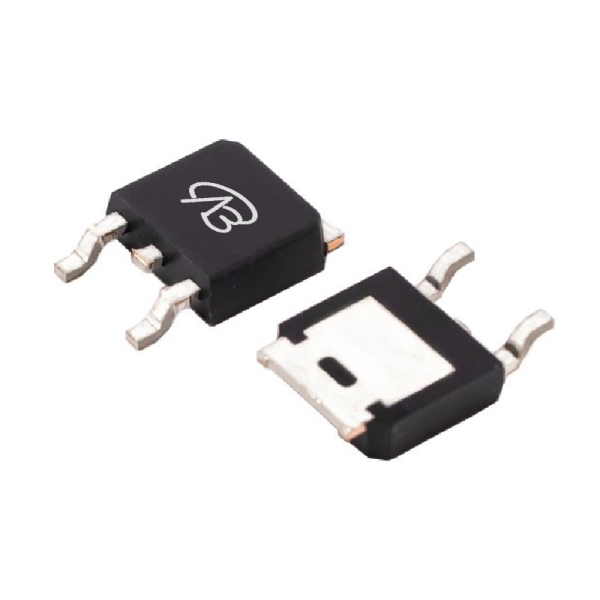
MOSFET Selection for High-Voltage & High-Current Applications: FCD360N65S3R0, SVD5865NLT4G vs. China Alternatives VBE16R10S, VBE1615
In today's power design landscape, balancing high voltage withstand, low conduction loss, and robust switching performance is a critical challenge for engineers. Selecting the right MOSFET goes beyond simple pin-to-pin substitution; it requires a careful trade-off among voltage rating, current capability, switching efficiency, and supply chain stability. This article uses two highly representative MOSFETs, FCD360N65S3R0 (650V N-channel) and SVD5865NLT4G (60V N-channel), as benchmarks. We will delve into their design cores and application scenarios, followed by a comparative evaluation of two domestic alternative solutions: VBE16R10S and VBE1615. By clarifying their parameter differences and performance orientations, we aim to provide a clear selection map to help you find the most suitable power switching solution for your next high-performance design.
Comparative Analysis: FCD360N65S3R0 (650V N-channel) vs. VBE16R10S
Analysis of the Original Model (FCD360N65S3R0) Core:
This is a 650V N-channel SUPERFET III MOSFET from onsemi, in a TO-252 (DPAK) package. Its design core leverages advanced superjunction (SJ) and charge balance technology to achieve an excellent combination of low on-resistance (360mΩ @10V) and low gate charge, minimizing both conduction and switching losses. A key advantage is its "Easy Drive" feature, which helps manage EMI and simplifies design implementation by withstanding high dv/dt rates. It is tailored for high-voltage, high-efficiency switching where managing switching noise and losses is paramount.
Compatibility and Differences of the Domestic Alternative (VBE16R10S):
VBsemi's VBE16R10S is also a Single N-channel MOSFET in a TO-252 package, offering a direct form-factor alternative. The main differences lie in the electrical parameters: VBE16R10S has a slightly lower voltage rating (600V vs. 650V) and a higher on-resistance (470mΩ @10V vs. 360mΩ). Its continuous drain current rating is similar at 10A.
Key Application Areas:
Original Model FCD360N65S3R0: Its high voltage rating and optimized switching performance make it ideal for high-voltage, efficiency-critical applications.
SMPS (Switch-Mode Power Supplies): PFC (Power Factor Correction) stages, flyback, or forward converters in AC-DC power supplies (e.g., for servers, industrial equipment).
Motor Drives: Inverter stages for high-voltage motor control.
Solar Inverters: Power switching in DC-AC conversion stages.
Alternative Model VBE16R10S: Suitable as a cost-effective alternative in applications where the full 650V rating is not strictly required, and a slightly higher conduction loss is acceptable. It fits well in 600V-system SMPS, lighting ballasts, or other medium-power off-line switchers.
Comparative Analysis: SVD5865NLT4G (60V N-channel) vs. VBE1615
This comparison shifts focus to high-current, low-voltage applications where minimizing conduction loss is the primary design pursuit.
Analysis of the Original Model (SVD5865NLT4G) Core:
This onsemi 60V N-channel MOSFET in a TO-252 package is engineered for high current and minimal conduction loss. Its core advantages are:
Excellent Conduction Performance: Very low on-resistance of 13mΩ @10V, enabling a high continuous drain current of 46A. This significantly reduces power loss in the on-state.
High Robustness: Features specified avalanche energy rating and is AEC-Q101 qualified, ensuring reliability in demanding environments like automotive.
Thermal Performance: With a power dissipation rating of 71W, the DPAK package offers good thermal capability for its current class.
Compatibility and Differences of the Domestic Alternative (VBE1615):
VBsemi's VBE1615 is a compelling "performance-enhanced" alternative in the same TO-252 package. It matches the 60V voltage rating but offers superior key parameters: a significantly higher continuous current of 58A and an even lower on-resistance of 10mΩ @10V (and 13mΩ @4.5V). This translates to potentially lower temperature rise and higher efficiency, especially in high-current applications.
Key Application Areas:
Original Model SVD5865NLT4G: Its low RDS(on) and high current capability make it an ideal choice for automotive and industrial high-current switching.
Automotive Systems: DC-DC converters, motor drives (e.g., fans, pumps), load switches, and solenoid drivers.
Power Tools: Motor control in battery-powered tools.
High-Current DC-DC Conversion: Synchronous buck converters for point-of-load (POL) regulation.
Alternative Model VBE1615: Is an excellent upgrade choice for applications demanding the utmost in current handling and lowest possible conduction loss. It is well-suited for next-generation, high-efficiency designs in areas like high-power motor drives, server VRMs, or any application where pushing the power density envelope is required.
Conclusion
In summary, this analysis reveals two distinct selection paths based on voltage domain:
For high-voltage (600-650V) applications like SMPS and inverters, the original FCD360N65S3R0, with its 650V rating, advanced SUPERFET III technology for low loss, and Easy Drive features, offers a high-performance, design-friendly solution. Its domestic alternative VBE16R10S provides a viable, cost-conscious option for 600V systems where the highest switching optimization is not critical.
For high-current, low-voltage (~60V) applications such as automotive and industrial power systems, the original SVD5865NLT4G sets a high standard with its low 13mΩ RDS(on), 46A current, and AEC-Q101 qualification. The domestic alternative VBE1615 emerges as a powerful "performance-plus" option, surpassing the original with 58A current and 10mΩ RDS(on), making it ideal for pushing efficiency and power density limits.
The core conclusion is that selection hinges on precise requirement matching. In an era of supply chain diversification, domestic alternatives like those from VBsemi not only provide reliable backup options but also offer compelling performance advantages in specific areas, giving engineers greater flexibility and resilience in design trade-offs and cost optimization. Understanding the design philosophy and parameter implications of each device is key to unlocking its full potential in your circuit.


 Download now