MOSFET Selection for Low-Power Signal and Dual-Channel Applications: BSS138LT1G, NTZD3152PT1G vs. China Alternatives VB162K, VBTA4250N
In the design of low-power circuits and space-constrained modules, selecting the right MOSFET for signal switching, level shifting, or compact power management is a critical task. This goes beyond simple part substitution, requiring careful balance among voltage rating, on-resistance, package size, and cost. This article uses two representative MOSFETs, BSS138LT1G (single N-channel) and NTZD3152PT1G (dual P-channel), as benchmarks. We will analyze their design focus and application scenarios, and comparatively evaluate two domestic alternative solutions, VB162K and VBTA4250N. By clarifying parameter differences and performance orientations, we aim to provide a clear selection guide for your next low-power or multi-channel design.
Comparative Analysis: BSS138LT1G (Single N-channel) vs. VB162K
Analysis of the Original Model (BSS138LT1G) Core:
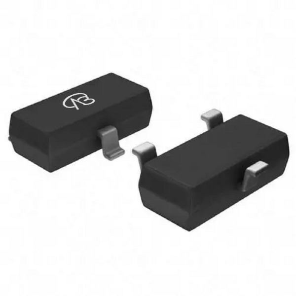
This is a 50V N-channel MOSFET from onsemi, housed in the ubiquitous SOT-23 package. Its design core is to provide reliable, low-threshold switching for low-power signal and power management applications. Key advantages include: a low gate threshold voltage (VGS(th) 0.5V-1.5V), making it suitable for low-voltage drive circuits (e.g., 3.3V, 2.5V logic). It features a continuous drain current of 200mA and an on-resistance of 5.6Ω at 2.75V VGS. It is AEC-Q101 qualified, making it suitable for automotive and other demanding applications requiring PPAP capability.
Compatibility and Differences of the Domestic Alternative (VB162K):
VBsemi's VB162K is offered in a compatible SOT23-3 package. The main differences lie in the electrical parameters: VB162K has a slightly higher voltage rating (60V vs. 50V) and a significantly lower on-resistance (2.8Ω @10V vs. 5.6Ω @2.75V, noting different test conditions). However, its continuous current rating (0.3A) is in a similar range to the original. The gate threshold is a standard 1.7V.
Key Application Areas:
Original Model BSS138LT1G: Its low threshold voltage and automotive-grade qualification make it ideal for precision low-voltage switching, especially in automotive electronics, portable devices, and battery-powered products. Typical applications include:
Low-side load switches in DC-DC converters.
Level translation circuits for logic interfaces.
Power management switches in computers, printers, and communication cards.
Alternative Model VB162K: More suitable for general-purpose low-power switching applications where a lower on-resistance and higher voltage margin are beneficial, but where the specific low VGS(th) or automotive qualification of the original is not strictly required.
Comparative Analysis: NTZD3152PT1G (Dual P-channel) vs. VBTA4250N
This dual P-channel MOSFET is designed for space-saving, dual high-side switching or complementary circuits in compact modules.
Analysis of the Original Model (NTZD3152PT1G) Core:
This onsemi part integrates two 20V P-channel MOSFETs in a tiny SOT-563 package. Its core advantages are:
Space Efficiency: Dual channels in a 6-pin package save significant board area.
Performance for Size: Offers a respectable continuous current of 430mA per channel and an on-resistance of 2Ω at a low 1.8V gate drive, enabling efficient switching from modern low-voltage microcontrollers.
Integrated Protection: Includes ESD protection, enhancing system robustness.
Compatibility and Differences of the Domestic Alternative (VBTA4250N):
VBsemi's VBTA4250N is a direct pin-to-pin compatible alternative in an SC75-6 package. It represents a significant performance enhancement in key parameters: while maintaining the same -20V voltage rating, it offers a much lower on-resistance (450mΩ @4.5V vs. 2Ω @1.8V) and a similar continuous current rating (-0.5A per channel). This translates to lower conduction losses and potentially better thermal performance.
Key Application Areas:
Original Model NTZD3152PT1G: Perfect for compact designs requiring dual high-side switches or complementary signal paths driven by low-voltage logic (e.g., 1.8V). Applications include:
Power switching for multiple peripheral modules or sensors.
Interface and bus switching circuits.
Portable device power management where board space is premium.
Alternative Model VBTA4250N: Better suited for applications where minimizing conduction loss in the dual P-channel switch is a priority, and where the gate drive voltage is typically 2.5V or higher, leveraging its superior RDS(on) performance.
Summary
This analysis reveals two distinct selection paths for low-power and multi-channel applications:
For single N-channel, low-threshold signal switching, particularly in automotive or precision low-voltage circuits, the original BSS138LT1G with its certified AEC-Q101 qualification and low VGS(th) remains a strong choice. Its domestic alternative VB162K offers a compatible package with generally lower RDS(on) and higher VDS, suitable for upgrades in general-purpose applications where those specific traits are valued.
For ultra-compact dual P-channel switching, the original NTZD3152PT1G excels in minimal footprint applications requiring operation from very low gate voltages (~1.8V). The domestic alternative VBTA4250N provides a compelling "performance-enhanced" option, delivering significantly lower on-resistance for higher efficiency in designs using standard 2.5V/3.3V or higher gate drive.
The core conclusion is: Selection hinges on precise requirement matching. In the landscape of supply chain diversification, domestic alternatives like VB162K and VBTA4250N not only provide reliable backup options but also offer performance advantages in key areas, granting engineers greater flexibility in design optimization and cost management. Understanding the specific design intent behind each device is paramount to unlocking its full potential in your circuit.


 Download now
 中文
中文 English
 Back to previous page


