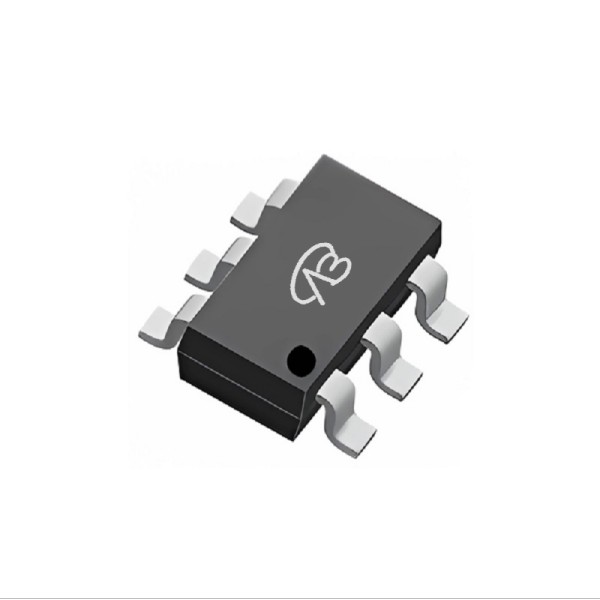
MOSFET Selection for Signal Switching & Power Management: BSS138BKS,115, PMV40UN2R vs. China Alternatives VBK362K, VB1330
In modern circuit design, selecting the right MOSFET for signal-level switching and compact power management is a critical task that balances performance, size, and cost. This article takes two representative MOSFETs—BSS138BKS,115 (Dual N-Channel) and PMV40UN2R (Single N-Channel)—as benchmarks. We will analyze their design cores and application scenarios, then evaluate the domestic alternative solutions VBK362K and VB1330 through a comparative parameter review. The goal is to provide a clear selection guide to help you find the optimal power switching component for your next design.
Comparative Analysis: BSS138BKS,115 (Dual N-Channel) vs. VBK362K
Analysis of the Original Model (BSS138BKS,115) Core:
This is a dual N-channel MOSFET from Nexperia in a compact TSSOP-6 (SOT-363) package. Its design core is to provide reliable signal switching and interface control in minimal board space. Key advantages include: a 60V drain-source voltage rating, a continuous drain current of 320mA per channel, and an on-resistance of 1.6Ω at 10V gate drive. It is optimized for low-power digital and analog switching.
Compatibility and Differences of the Domestic Alternative (VBK362K):
VBsemi's VBK362K is also a dual N-channel MOSFET in an SC70-6 package, offering a similar small-footprint solution. It is pin-to-pin compatible in many layouts. The main differences are in electrical parameters: VBK362K matches the 60V voltage rating but offers a slightly lower continuous current of 0.3A (300mA). Its on-resistance is higher at 2.5Ω (at 10V), compared to the original's 1.6Ω.
Key Application Areas:
Original Model BSS138BKS,115: Ideal for space-constrained applications requiring dual-channel signal isolation or switching with moderate current handling. Typical uses include:
Level translation and interface protection in communication modules (UART, I2C, GPIO).
Load switching for sensors, LEDs, or other low-power peripherals in portable/IoT devices.
Signal multiplexing and routing in analog/digital systems.
Alternative Model VBK362K: A suitable alternative for applications where the 60V rating is required but the switching current is below 300mA. It fits well in cost-sensitive designs needing dual N-channel functionality in a tiny package.
Comparative Analysis: PMV40UN2R (N-channel) vs. VB1330
This comparison shifts to single N-channel MOSFETs designed for higher current handling in a popular miniature package.
Analysis of the Original Model (PMV40UN2R) Core:
This Nexperia MOSFET in SOT-23 package balances performance and size. Its core advantages are:
Solid Power Handling: With a 30V rating, it supports a continuous drain current of 3.7A.
Low Conduction Loss: Features an on-resistance of 44mΩ at a 4.5V gate drive, ensuring good efficiency for its size.
Proven Miniature Package: The SOT-23 (TO-236AB) is industry-standard, offering a good compromise between footprint and thermal performance for moderate power.
Compatibility and Differences of the Domestic Alternative (VB1330):
VBsemi's VB1330 is a direct SOT-23 pin-to-pin compatible alternative that offers performance enhancement in key areas:
It matches the 30V drain-source voltage.
It provides a significantly higher continuous current rating of 6.5A.
It features a lower on-resistance of 33mΩ at 4.5V (and 30mΩ at 10V), promising reduced conduction losses and lower temperature rise.
Key Application Areas:
Original Model PMV40UN2R: An excellent choice for efficient power switching and management in compact 12V-24V systems where board space is premium. Common applications include:
Power switch for USB ports, peripheral power rails, or subsystem power gating.
Low-side switch in DC-DC converters for point-of-load regulation.
Driver for small motors, solenoids, or relays.
Alternative Model VB1330: Better suited for upgraded scenarios demanding higher current capability and lower losses within the same SOT-23 footprint. Ideal for:
More demanding power path management requiring higher current headroom.
DC-DC converter designs where lower RDS(on) directly improves efficiency.
Driving loads up to 6.5A where the original part's 3.7A limit is insufficient.
Summary and Selection Paths:
This analysis reveals two distinct selection strategies:
1. For Dual N-Channel Signal Switching: The original BSS138BKS,115 offers a balanced performance of 60V rating, 320mA current, and 1.6Ω RDS(on) in a TSSOP-6 package, making it a reliable choice for interface control and low-power switching. Its domestic alternative VBK362K provides package compatibility and the same voltage rating but is tailored for applications where the current requirement is under 300mA and cost is a primary driver.
2. For Single N-Channel Power Switching: The original PMV40UN2R delivers a robust 3.7A capability with 44mΩ RDS(on) in the ubiquitous SOT-23 package, serving as a versatile workhorse for numerous power management tasks. The domestic alternative VB1330 emerges as a performance-upgrade option, offering substantially higher current (6.5A) and lower on-resistance (33mΩ) in the same package, enabling higher power density and efficiency for next-generation designs.
Core Conclusion: The choice is not about absolute superiority but precise requirement matching. In the era of supply chain diversification, domestic alternatives like VBK362K and VB1330 provide not only viable backups but also opportunities for cost optimization and, in cases like the VB1330, significant performance gains. Understanding the parameter nuances and design intent behind each MOSFET is key to unlocking its full potential in your circuit.


 Download now