MOSFET Selection for Automotive and High-Power Applications: DMN6010SCTBQ-13, DMN601VKQ-7 vs. China Alternatives VBL1606, VBTA3615M
In the demanding fields of automotive electronics and high-power switching, selecting a MOSFET that delivers robust performance, reliability, and cost-effectiveness is a critical engineering challenge. This goes beyond simple part substitution, requiring a careful balance of current handling, on-resistance, package suitability, and qualification standards. This article uses two distinct MOSFETs from DIODES, the high-power DMN6010SCTBQ-13 (Single N-channel) and the automotive-grade dual N-channel DMN601VKQ-7, as benchmarks. We will deeply analyze their design cores and application contexts, and provide a comparative evaluation of their Chinese alternative solutions, VBL1606 and VBTA3615M. By clarifying their parameter differences and performance orientations, we aim to offer a clear selection guide to help you find the optimal power switching solution for your next design.
Comparative Analysis: DMN6010SCTBQ-13 (Single N-channel) vs. VBL1606
Analysis of the Original Model (DMN6010SCTBQ-13) Core:
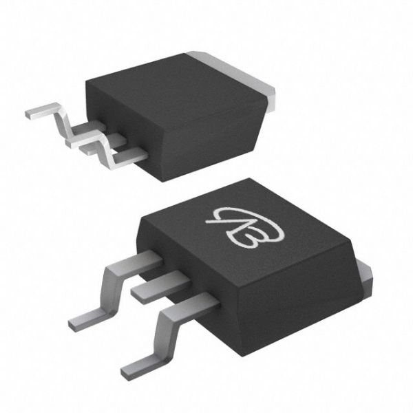
This is a 60V, single N-channel MOSFET from DIODES in a TO-263AB (D2PAK) package. Its design core is to provide a high-current, low-loss switching solution in a standard power package. Key advantages include a very high continuous drain current rating of 128A and a low on-resistance (RDS(on)) of 10mΩ measured at 10V, 25A. This combination makes it suitable for applications where minimizing conduction loss under high current is paramount.
Compatibility and Differences of the Domestic Alternative (VBL1606):
VBsemi's VBL1606 is a direct pin-to-pin compatible alternative in the same TO-263 package. It represents a significant performance enhancement in key electrical parameters: while maintaining the same 60V voltage rating, it offers a dramatically lower on-resistance of 4mΩ (@10V) and a higher continuous current rating of 150A. This translates to potentially lower conduction losses and higher current handling capability in similar applications.
Key Application Areas:
Original Model DMN6010SCTBQ-13: Ideal for high-current switching and power conversion stages where its 128A capability and 10mΩ RDS(on) provide solid performance. Typical applications include:
High-current DC-DC converters and voltage regulators.
Power management in industrial equipment, motor drives, and power supplies.
Load switches and battery protection circuits for high-power systems.
Alternative Model VBL1606: More suitable for upgraded scenarios demanding even lower conduction losses, higher efficiency, or greater current margin. It is an excellent choice for next-generation designs or for enhancing the thermal and efficiency performance of existing applications based on the original part.
Comparative Analysis: DMN601VKQ-7 (Dual N-channel) vs. VBTA3615M
This comparison shifts focus to compact, automotive-qualified signal-level switching. The design pursuit for DMN601VKQ-7 is miniaturization and reliability for automotive environments.
Analysis of the Original Model (DMN601VKQ-7) Core:
This is a 60V, dual N-channel MOSFET from DIODES in an ultra-small SOT-563 package. It is specifically designed to meet the stringent requirements of automotive applications, being AEC-Q101 qualified with PPAP documentation available. Its core advantages are its dual-channel integration in a tiny footprint, making it perfect for space-constrained automotive modules. It features a continuous drain current of 305mA per channel and an on-resistance of 1.3Ω (@10V), suitable for low-current switching and interface control.
Compatibility and Differences of the Domestic Alternative (VBTA3615M):
VBsemi's VBTA3615M is a direct pin-to-pin compatible alternative in the same SC75-6 (similar to SOT-563) package. It is also a dual N-channel device with the same 60V rating. The key differences lie in its detailed specifications: it lists RDS(on) at two gate drives (1500mΩ @4.5V and 1200mΩ @10V) and a slightly lower continuous current rating of 0.3A (300mA). It serves as a functional and package-compatible alternative for automotive and general-purpose low-power dual switching needs.
Key Application Areas:
Original Model DMN601VKQ-7: Its AEC-Q101 qualification and dual-channel design make it an ideal choice for automotive electronic control units (ECUs) and compact interface switching. Typical applications include:
General-purpose interface switches in automotive body control modules, infotainment systems, and sensor interfaces.
Load switching for low-power peripherals in space-constrained, reliability-focused environments.
Alternative Model VBTA3615M: Provides a viable domestic alternative for dual N-channel switching applications requiring 60V rating in a miniaturized package. It is suitable for both automotive (where qualification is verified) and industrial/commercial low-power interface switching, offering supply chain diversification.
Summary
In summary, this analysis reveals two distinct selection paths based on power level and application focus:
For high-power, high-current switching, the original model DMN6010SCTBQ-13 provides a solid solution with 128A current and 10mΩ RDS(on). Its domestic alternative VBL1606 offers a compelling performance-upgraded path with significantly lower RDS(on) (4mΩ) and higher current (150A), enabling higher efficiency and power density in new designs or upgrades.
For compact, automotive-grade, low-power dual-channel switching, the original AEC-Q101 qualified DMN601VKQ-7 is tailored for reliable automotive interface control. Its domestic alternative VBTA3615M provides a package-compatible and functionally equivalent option for dual N-channel switching needs, supporting supply chain resilience.
The core conclusion is that selection hinges on precise requirement matching. In the context of supply chain diversification, domestic alternatives not only provide reliable backup options but can also offer performance enhancements or cost benefits, giving engineers greater flexibility in design trade-offs and component sourcing. Understanding the specific design intent and parameter implications of each device is key to unlocking its full value in the circuit.


 Download now
 中文
中文 English
 Back to previous page


