MOSFET Selection for Power Management and High-Current Applications: DMN3015LSD-13, DMNH6010SCTB-13 vs. China Alternatives VBA3310, VBL1606
In modern power design, engineers must balance performance, efficiency, and cost. This article takes two representative MOSFETs—DMN3015LSD-13 (dual N‑channel) and DMNH6010SCTB‑13 (high‑current N‑channel)—as benchmarks, analyzes their design focus and application scenarios, and evaluates two domestic alternatives, VBA3310 and VBL1606. By comparing parameter differences and performance orientation, we provide a clear selection guide for your next power‑switching solution.
Comparative Analysis: DMN3015LSD‑13 (Dual N‑channel) vs. VBA3310
Analysis of the Original Model (DMN3015LSD‑13) Core:
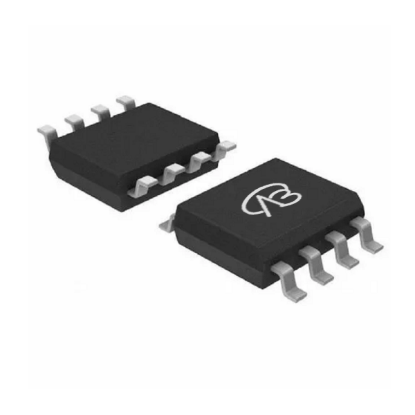
This is a dual N‑channel MOSFET from DIODES in an SO‑8 package. Its design aims to minimize conduction loss while maintaining excellent switching performance, making it ideal for efficient power‑management applications. Key advantages include a low on‑resistance of 18 mΩ at 4.5 V gate drive and a continuous drain current of 8.4 A per channel.
Compatibility and Differences of the Domestic Alternative (VBA3310):
VBsemi’s VBA3310 is a dual N‑channel MOSFET in the same SOP‑8 package, offering pin‑to‑pin compatibility. It provides improved electrical parameters: the same 30 V voltage rating but lower on‑resistance—12 mΩ at 4.5 V and 10 mΩ at 10 V—and a higher continuous current rating of 13.5 A per channel.
Key Application Areas:
Original Model DMN3015LSD‑13: Well‑suited for compact, efficiency‑critical power‑management circuits such as synchronous rectification in DC‑DC converters, load‑switch arrays, and multi‑channel power distribution in 12 V/24 V systems.
Alternative Model VBA3310: Offers enhanced conduction performance and higher current capability, making it a superior drop‑in replacement for applications demanding lower loss and higher power density within the same voltage range.
Comparative Analysis: DMNH6010SCTB‑13 (High‑Current N‑channel) vs. VBL1606
Analysis of the Original Model (DMNH6010SCTB‑13) Core:
This is a high‑power N‑channel MOSFET in a TO‑263AB (D2PAK) package. Designed for high‑current applications, it features a 60 V drain‑source voltage, a continuous current rating of 133 A, and an on‑resistance of 10 mΩ at 10 V, 25 A. Its robust package provides excellent thermal performance for demanding power stages.
Compatibility and Differences of the Domestic Alternative (VBL1606):
VBsemi’s VBL1606 is a direct alternative in the same TO‑263 package. It matches the 60 V rating but significantly outperforms the original in key parameters: an ultra‑low on‑resistance of 4 mΩ at 10 V and a higher continuous current rating of 150 A.
Key Application Areas:
Original Model DMNH6010SCTB‑13: Ideal for high‑current switching applications such as motor drives, high‑power DC‑DC converters (e.g., in server/telecom power supplies), and industrial power‑stage designs where thermal management is critical.
Alternative Model VBL1606: With its lower on‑resistance and higher current capability, it is an excellent performance‑upgrade choice for applications requiring minimized conduction losses, higher efficiency, and increased power handling, such as advanced motor drives and high‑density power converters.
Conclusion
This comparison reveals two distinct selection paths:
- For dual N‑channel applications in compact power management, the original DMN3015LSD‑13 offers a balanced performance profile. Its domestic alternative VBA3310 provides a compatible, enhanced‑performance solution with lower RDS(on) and higher current capability.
- For high‑current, high‑voltage applications, the original DMNH6010SCTB‑13 delivers robust performance in a thermally efficient package. The domestic alternative VBL1606 achieves significant performance gains with ultra‑low RDS(on) and higher current rating, enabling higher efficiency and power density.
The core insight is that selection depends on precise requirement matching. Domestic alternatives not only offer reliable backup options but also provide parameter advancements, giving engineers greater flexibility in design trade‑offs and cost control. Understanding each device’s design philosophy and parameter implications is key to maximizing its value in your circuit.


 Download now