MOSFET Selection for Compact Power Management: DMG2301L-7, DMP2240UDM-7 vs. China Alternatives VB2212N, VB4290
In modern power design, selecting the right MOSFET for space-constrained and efficiency-driven applications is a critical task for engineers. It involves balancing performance, size, cost, and supply chain stability. This article takes two representative MOSFETs—DMG2301L-7 (single P-channel) and DMP2240UDM-7 (dual P-channel)—as benchmarks, analyzes their design focus and application scenarios, and evaluates two domestic alternative solutions, VB2212N and VB4290. By comparing parameter differences and performance orientations, we provide a clear selection guide to help you find the most suitable power switching solution.
Comparative Analysis: DMG2301L-7 (Single P-channel) vs. VB2212N
Analysis of the Original Model (DMG2301L-7) Core:
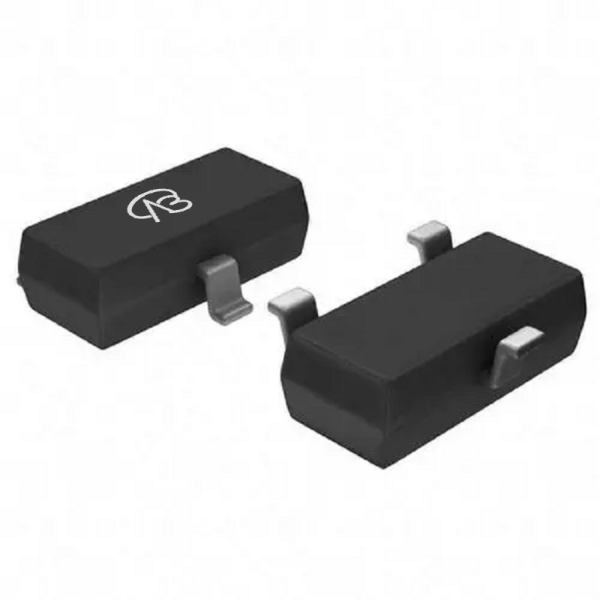
This is a 20V P-channel MOSFET from DIODES in a compact SOT-23 package. It is designed to minimize on-resistance (RDS(ON)) while maintaining excellent switching performance, making it ideal for high-efficiency power management. Key advantages include a continuous drain current of 3A and an on-resistance of 150mΩ at 2.5V gate drive.
Compatibility and Differences of the Domestic Alternative (VB2212N):
VBsemi’s VB2212N is a pin-to-pin compatible alternative in SOT-23 package. It offers improved electrical parameters: lower on-resistance of 90mΩ at 4.5V and 71mΩ at 10V, with a similar voltage rating (-20V) and continuous current (-3.5A). This provides better conduction loss and efficiency in compatible applications.
Key Application Areas:
- Original Model DMG2301L-7: Suitable for low-power, space-sensitive applications such as load switching in portable devices, power management in battery-operated systems, and DC-DC conversion in compact designs.
- Alternative Model VB2212N: Ideal for upgrades where lower on-resistance and higher efficiency are needed within the same voltage and current range, such as enhanced power switches or efficient voltage regulators.
Comparative Analysis: DMP2240UDM-7 (Dual P-channel) vs. VB4290
Analysis of the Original Model (DMP2240UDM-7) Core:
This dual P-channel MOSFET from DIODES in SOT-26 package is designed for applications requiring two switches in minimal space. It features low on-resistance (150mΩ at -4.5V), low gate threshold voltage (≤1V), fast switching, and compliance with AEC-Q101 for high reliability. It supports up to 2A continuous current per channel.
Compatibility and Differences of the Domestic Alternative (VB4290):
VBsemi’s VB4290 is a direct alternative in SOT-23-6 package with enhanced performance. It offers significantly lower on-resistance: 100mΩ at 2.5V and 75mΩ at 4.5V, with higher continuous current (-4A total) and similar voltage rating (-20V). This results in better power handling and reduced losses.
Key Application Areas:
- Original Model DMP2240UDM-7: Excellent for dual-switch applications like power distribution, battery protection circuits, and interface switching in consumer electronics, where reliability and compact size are critical.
- Alternative Model VB4290: Suited for higher-performance needs, such as compact power modules, advanced battery management, or systems requiring lower conduction loss and higher current capacity.
Conclusion:
This comparison highlights two clear selection paths:
- For single P-channel applications in tight spaces, the original DMG2301L-7 offers a balanced mix of low RDS(ON) and switching performance. Its alternative VB2212N provides a compatible upgrade with lower on-resistance for improved efficiency.
- For dual P-channel designs, the original DMP2240UDM-7 delivers reliable, AEC-Q101-compliant switching in a tiny footprint. The alternative VB4290 enhances performance with lower RDS(ON) and higher current capability, ideal for more demanding power tasks.
The core insight: Selection depends on precise requirement matching. Domestic alternatives like VB2212N and VB4290 not only offer reliable backups but also enable performance gains, giving engineers greater flexibility in design trade-offs and cost optimization. Understanding each device’s design intent and parameters is key to maximizing circuit value.


 Download now
 中文
中文 English
 Back to previous page


