For the driving circuit of the MOS tube of a small power supply (less than 50W), usually only one driving resistor Rg is needed to complete the driving, and at this time, the resistance values of the driving turn-on resistor and the turn-off resistor are the same.
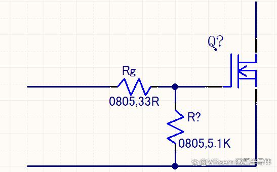
If the power supply is small or medium (50W to 500W) and has certain efficiency design requirements, the on-resistance Rg(on) and the off-resistance Rg(off) need to be separated. Generally, the following two designs are adopted.
The first design method is Rg(on)=Rg1+Rg2, Rg(off)=Rg1.
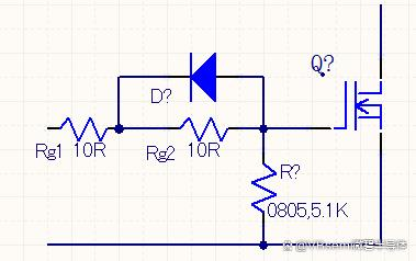
The second design method separates Rg(on) and Rg(off) for easy adjustment.
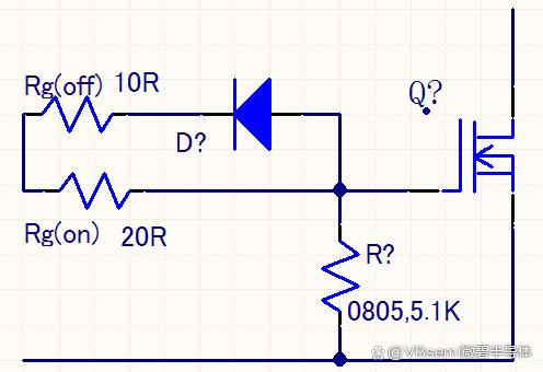
For medium power supply (300W to 1500K), not only the on-resistance and off-resistance need to be separated, but also the driving Miller platform needs to be processed. Generally, a set of RC circuits is added between the GS of the MOS tube, and the oscillation problem in the Miller platform of the MOS tube is adjusted by adjusting the RC parameters. The specific parameters need to be determined according to the circuit and MOS tube selection and debugging.
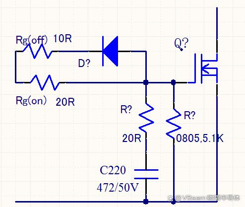
For medium to high power power supplies (1200W to 5KW or even 10KW), the driver design is closely related to MOS tube selection, parasitic parameters, power routing and other aspects.
There are several main ideas in MOS tube driver design:
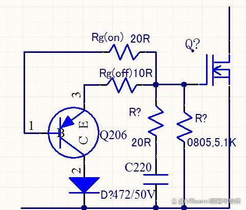
First, use the transistor to directly pull the G level to the S level when the driver is turned off to reduce the drive shutdown loop and enhance the anti-interference ability.
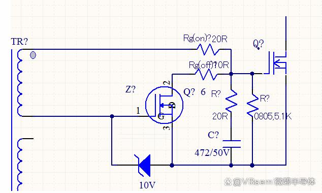
The second is to use NMOS to directly pull the G level to the S level when the driver is turned off to achieve the same effect;
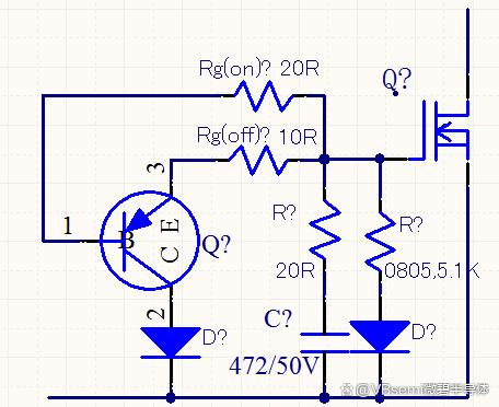
The third is to use the transistor to pull the G level to the S level when the drive is turned off, and at the same time connect a diode in series with the GS resistor to further enhance the anti-interference ability of the drive circuit.
In the driver design, power circuit interference must be reduced or avoided, and signal processing must be performed at the driver drive signal input source to prevent interference signals from coupling into the real signal .
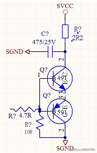
Specifically, a totem pole can be used as a driver . (Low cost, suitable for small and medium power and cost-sensitive products)
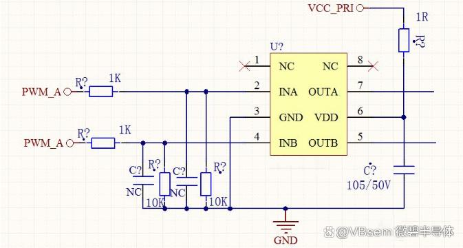
Or use a driver IC as a driver to drive the MOS or drive the transformer (suitable for designs with higher power and longer drive lines), and add a pull-down resistor and RC filtering at the signal input end to ensure a clean signal and enhance anti-interference capabilities.
In the process of power supply debugging, the debugging of driving signal is very important, which directly affects the reliability, efficiency, design temperature rise and EMC characteristics of the power supply. Therefore, the design of driving circuit is an important indicator of power supply design, and the rationality of driving parameters has a direct impact on all aspects of power supply performance.
*To request free samples, please complete and submit the following information.
Our team will review your application within 24 hours and arrange shipment upon approval. Thank you!