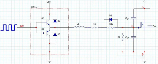
Take this driver circuit that can control the switching speed as an example.

As shown in the figure, D1 is a fast recovery diode connected in parallel to the driving resistor Rg2, which reduces the turn-off time and the turn-off loss. Rg1 can limit the turn-off current. R1 is the pull-down resistor of the gate source of the MOSFET, which provides a discharge circuit for the charge accumulated on the gate of the MOSFET. (According to the high input impedance of the MOSFET gate, a little static electricity or interference may cause the MOS tube to be mis-conducted, so R1 also plays a role in reducing the input impedance, and the value is generally between 10k and tens of k)
Lp is the stray parasitic inductance of the driver trace, including the inductive reactance of the driver IC pins, MOS pins, and PCB traces. The exact value is difficult to determine and is usually taken as tens of nH.
Calculation of driving resistance Rg:
The parasitic inductance of the driving trace and the junction capacitance of the MOS tube will form an LC oscillation circuit. If the output end of the driving chip is directly connected to the gate, large oscillations will be generated at the rising and falling edges of the PWM wave, causing the MOS tube to heat up rapidly or even explode. The general solution is to connect a resistor in series with the gate to reduce the Q value of the LC oscillation circuit and make the oscillation decay rapidly.
Driving resistance lower limit:
When the MOS is turned on, Vcc charges Ciss=Cgs+Cgd through the driving resistor, as shown in the figure above (ignore the effect of the pull-down resistor R1). According to the LC oscillation circuit model, the corresponding equation of the loop in the complex frequency domain can be listed.

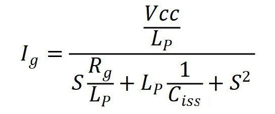
Solve for I g and transform it into a typical second-order system

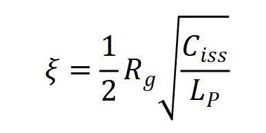
Then solve the damping coefficient of the second-order system based on the LC oscillation circuit

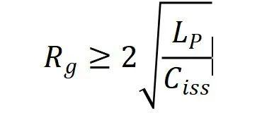
Then according to the characteristics of the LC oscillation circuit, in order to ensure that the driving current ig does not oscillate, the system must be in an overdamped state; that is, the damping ratio must be greater than 1, then the equation is solved to obtain the lower limit range of Rg=Rg1+Rg2

Driver off resistance upper limit:
When the MOS tube is turned off, the high dv/dt generated by Vds will cause the parasitic capacitor Cgd to discharge and form a large current (Ic=Cdv/dt). This current Igd flows through the driving resistor Rg, generating a voltage Vgoff=IgdxRg between GS. To prevent mis-conduction, Vgoff cannot exceed the MOS conduction threshold voltage Vth.
Then list the inequalities

Then the upper limit of the driving resistance Rgoff = Rg1 is obtained.

In actual design, the lower limit of Rg1+Rg2 is calculated to avoid drive current oscillation, and then the upper limit of Rg1 is determined to prevent false turn-on during shutdown. Finally, the ideal drive resistance parameters are determined through experimental debugging and optimization, taking into account factors such as loss, electromagnetic interference (EMI), and bridge topology dead zone control.
*To request free samples, please complete and submit the following information.
Our team will review your application within 24 hours and arrange shipment upon approval. Thank you!