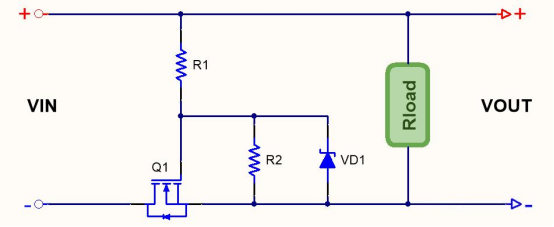
In the design of power reverse connection protection circuit, although the diode can use the unidirectional conduction characteristic to prevent the power reverse connection from damaging the circuit, the tube voltage drop problem leads to large losses. MOS tube has the excellent characteristic of low conduction voltage drop, so how to use this excellent characteristic of MOS tube to design the reverse connection protection circuit?

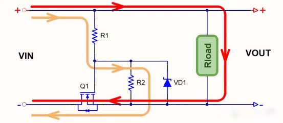
Taking NMOS as an example, when the power input is positive at the top and negative at the bottom, the current path shown by the yellow line in the figure below passes through R1, R2 and the MOS parasitic diode and then reaches the ground. At this time, the voltage divider of R1 and R2 makes the GS pole voltage greater than the MOS conduction voltage Vgs, so that the MOS tube is turned on, and the entire circuit loop shown by the red line is connected, and the circuit works normally.

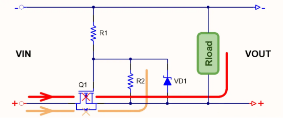
When the input is negative at the top and positive at the bottom, the current path shown by the yellow line is reversely cut off because the MOS parasitic diode is reversely cut off, and the GS pole of the MOS tube is cut off without voltage, the entire circuit loop is disconnected, and the system circuit is effectively protected.

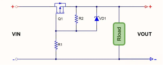
For PMOS reverse connection protection circuit, its reverse connection protection principle is similar to that of NMOS.

But it should be noted that usually, if the circuit system has a common ground, PMOS is used to prevent reverse connection, and if the circuit system has a common source, NMOS is used to prevent reverse connection.
*To request free samples, please complete and submit the following information.
Our team will review your application within 24 hours and arrange shipment upon approval. Thank you!