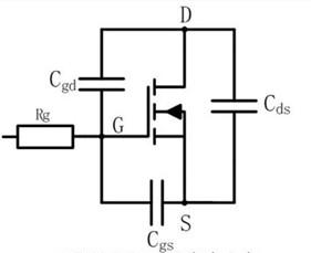
In the circuit, there is junction capacitance between DG and GS of the MOS tube. When the circuit is working, the voltage between DS will charge these junction capacitances.

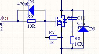
As the static voltage accumulated at the G pole continues to increase, once it reaches a certain level, the MOS tube will be turned on. If the voltage is too high, it may even damage the MOS tube. At this time, R7 provides a discharge channel for the junction capacitance and can speed up the MOS switching speed. Its resistance is generally around several thousand ohms.

When the MOS tube is turned off, the loop formed by R6 and D3 can quickly discharge the charge of the gate junction capacitance, causing the gate potential to drop rapidly, thereby accelerating the switching speed of the MOS tube. In addition, in a high-frequency environment, the input impedance of the MOSFET will decrease, and it will become a negative resistance within a specific frequency range and cause oscillation. At this time, R6 can reduce the oscillation. The resistance value of R6 is generally small, usually between a few ohms and tens of ohms.
In addition, due to the distributed inductance of the MOS tube, a reverse peak voltage will be generated when it is turned off. The Rc part is used to absorb the spike wave and provide a release loop for the reverse peak voltage. In addition, D5 can protect the MOS tube when the reverse peak voltage occurs, preventing it from being broken down by excessive voltage. According to experiments, if the loop composed of C11, R8 and D5 is removed, the waveform of the circuit will fluctuate greatly.
*To request free samples, please complete and submit the following information.
Our team will review your application within 24 hours and arrange shipment upon approval. Thank you!