In the ideal state when driving the MOS tube, the gate drive waveform of the MOS tube is a relatively smooth pulse signal.

Ideal square wave

Actual square wave
However, the Ugs waveform actually measured often has oscillations, which will cause noise interference and additional power loss.

Do you know why oscillation occurs?
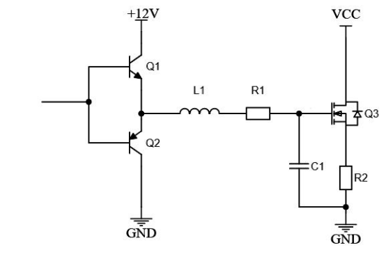
(As shown in the figure) In order to provide enough driving current to the MOS tube, a push-pull circuit is generally used, such as transistors Q1 and Q2. In the actual circuit, there will be inductive reactance and resistance, such as the equivalent inductance L1 and equivalent resistance R1 in the figure, and there is a parasitic capacitance (equivalent to C1) between the MOS tubes GD and GS. L1 and C1 form a resonant oscillation circuit. Because R1 is extremely small and cannot play a damping role, an oscillating waveform is formed at the rising and falling edges of the driving pulse.
In order to suppress oscillation, a driving resistor is usually connected in series with the gate, and the resistor should be as close to the gate as possible when routing on the PCB. The value of the gate driving resistor has an impact on the oscillation:
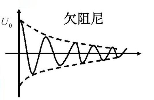
When the gate is turned on, the driving resistance is too small (underdamped state), and the oscillation cannot be suppressed;

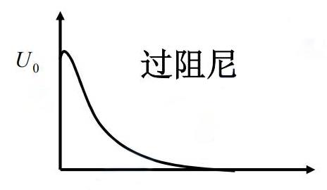
When the value is too large (over-damping state), the MOS tube is turned on for a long time and the switching loss is large.

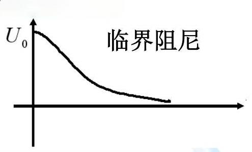
Therefore, the most ideal state is the critical damping state, in which the gate drive resistor can suppress the oscillation without prolonging the MOS tube turn-on time.

At the same time, when designing the PCB, the gate connection trace should be as short as possible and without bends to reduce the oscillation of the drive pulse waveform and the parasitic inductance value.
*To request free samples, please complete and submit the following information.
Our team will review your application within 24 hours and arrange shipment upon approval. Thank you!