Today I will share a PMOS circuit design and learn in detail about the role of each component in the circuit.

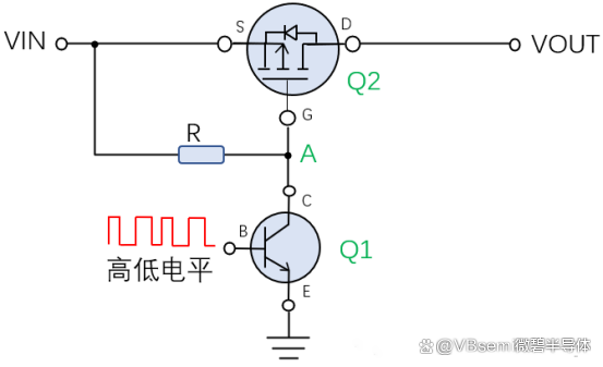
Here, Q1 is an NPN transistor, Q2 is a PMOS transistor, and the MCU controls the on and off of the transistor Q1 through high and low levels.
When Q1 is turned off, since no current flows through the resistor R, the voltage at point A is equal to Vin, that is, the gate voltage VG of Q2 is equal to Vin. At this time, the source voltage VS of Q2 is also equal to Vin, and the voltage across G and S of Q2 is equal to 0. Q2 is turned off, and the VOUT output is turned off at this time.
When Q1 is turned on, the voltage at point A is 0. At this time, the G and S voltages of Q2 are 0-Vin=-Vin. When -Vin meets the turn-on threshold voltage of the PMOS tube of Q2, Q2 is turned on, which means that the Vout output is turned on.
Switching tube Q1
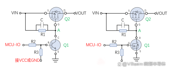
You can choose NMOS or NPN transistors. According to the IO voltage of the MCU, the turn-on voltage of the MOS tube should be greater than the turn-on voltage of the transistor.

Current limiting resistor R2
The value of R2 should be selected according to the MCU's IO voltage, maximum output current and the type of switch tube Q1. The current limiting resistor of the MOS tube can usually be at the level of tens of Ω. The current limiting resistor of the transistor should be calculated based on the MCU's IO voltage/maximum output current, which is generally at the kΩ level.
Upper and lower resistors R3
R3 can be used as a pull-up resistor or a pull-down resistor.
This is determined by the default state of VOUT. When powered on, the MCU is not ready yet, so a resistor is needed to fix the voltage level. If VOUT is powered on by default, R3 needs to be pulled up, otherwise it needs to be pulled down.
The pull-up voltage VCC is the IO power supply voltage of the MCU.
GS parallel capacitor C
A capacitor C is connected in parallel between the GS of the PMOS. When the PMOS is turned on, the capacitor C is charged first. At this time, the VGS of the PMOS starts to rise from 0, and the PMOS passes through the variable resistor and then reaches the saturation region, which can prevent various factors in the subsequent circuit at the moment of turning on, causing the PMOS to be impacted by a large current.
GS resistor R1
The value of R1 is tens or hundreds of KΩ, which can effectively reduce the power consumption of Q1 when it is turned on. However, it should be noted that R1 provides a discharge circuit for the GS capacitor of MOS. If R1 is too large, the MOS tube will be turned off more slowly.
That’s all for today.


Some of the above pictures are from the Internet
*To request free samples, please complete and submit the following information.
Our team will review your application within 24 hours and arrange shipment upon approval. Thank you!