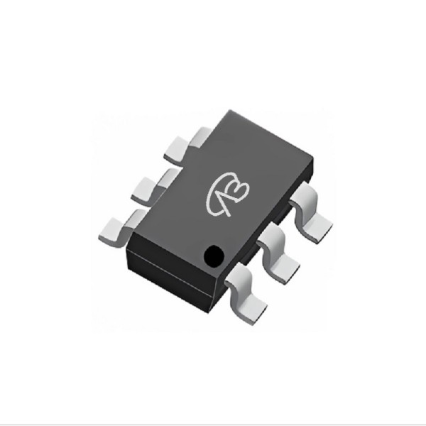
Product parameter:
| VB Package |
Configuration |
VDS(V) |
VGS |
Vthyp(V) |
ID(A) |
Rds2.5 |
Rds4.5 |
Rds10 |
Technology |
| SC70-6 |
Dual-N+N |
20V |
|
0.5~1.5V |
2.6A |
110mΩ |
|
|
Trench |
| VB Package |
Configuration |
VCE |
VGE |
VGEth(V) |
VCEsat15V |
ICE |
Technology |
| SC70-6 |
Dual-N+N |
|
|
|
|
|
Trench |
| VB Package |
Configuration |
VDS(V) |
VGS |
Vthyp(V) |
ID(A) |
Rds18 |
Technology |
| SC70-6 |
Dual-N+N |
20V |
|
0.5~1.5V |
2.6A |
|
Trench |
| VB Package |
Configuration |
VDS(V) |
VGS |
Vthyp(V) |
ID(A) |
Rds6 |
Technology |
| SC70-6 |
Dual-N+N |
20V |
|
0.5~1.5V |
2.6A |
|
Trench |
| VB Package |
Polarity |
Vz / VR |
Pd |
VF |
IF |
IR |
Cd |
Type |
| SC70-6 |
Dual-N+N |
|
|
|
|
|
|
|
**SSM6N39TU-VB MOSFET detailed parameter description**
- **Package**: SC70-6
- **Configuration**: Dual-N+N-Channel
- **Drain-source voltage (VDS)**: 20V
- **Gate-source voltage (VGS)**: ±12V
- **Throw-on voltage (Vth)**: 0.5V ~ 1.5V
- **On-resistance (RDS(ON))**:
- 110mΩ (VGS = 2.5V)
- 86mΩ (VGS = 4.5V)
- **Maximum drain current (ID)**: 2.6A
- **Operating temperature range**: -55°C to 150°C
- **Technology**: Trench
- **Maximum power loss (Pd)**: Depends on operating conditions and application requirements
- **Junction temperature (Tj)**: Maximum 150°C
- **Gate charge (Qg)**: Suitable for high-frequency switching applications
- **Thermal resistance (RθJA)**: Calculated based on actual heat dissipation design, usually below 200°C/W
Domain and module applications:
**Application fields and modules of SSM6N39TU-VB**
1. **Low-power power management system**:
Due to its low on-resistance, SSM6N39TU-VB is very suitable for low-power power management modules, especially in miniaturized devices such as mobile phones, portable electronic devices and sensor systems. These systems have strict requirements for efficient power conversion and energy management. The high efficiency of SSM6N39TU-VB can significantly extend battery life and reduce energy loss.
2. **DC-DC converter**:
In DC-DC converter applications, SSM6N39TU-VB can be used as a power switching element, especially in miniaturized, high-frequency conversion applications. By using this MOSFET, designers can improve conversion efficiency and maintain low power loss under a wider range of load conditions, suitable for various power supply voltage adjustments, such as 5V/3.3V, 12V/5V conversion, etc.
3. **Load switch applications**:
The dual N-Channel configuration of SSM6N39TU-VB makes it very useful in load switching and current management circuits. By controlling the on/off state of the load, it can provide efficient load switching and is widely used in consumer electronic devices, automotive electronics and industrial control, such as battery protection circuits, switching power supplies, low-power modules, etc.
4. **LED driver power supply**:
In LED driver power supply modules, SSM6N39TU-VB can be used to efficiently control current to ensure that the battery or power supply can stably drive the LED light. Its low on-resistance characteristics can effectively reduce power loss while improving the overall efficiency of the system, and is suitable for power drive of various lighting systems and display panels.
5. **Automotive electronic systems**:
In the field of automotive electronics, SSM6N39TU-VB can be used in battery management systems (BMS), especially in battery protection and power regulation circuits in electric vehicles (EV) and hybrid electric vehicles (HEV). This MOSFET can handle high-frequency switching operations and high-current loads, and has excellent thermal performance, ensuring stable operation even in high-temperature environments.
6. **Wireless communication module**:
Due to its fast switching and low on-resistance characteristics, the SSM6N39TU-VB is also very suitable for power management and signal switching in wireless communication modules. It can effectively reduce signal loss and improve data transmission efficiency, and is suitable for wireless communication devices such as Wi-Fi, Bluetooth and Zigbee in the 2.4GHz frequency band.
7. **Load protection circuit**:
In low-power devices, the SSM6N39TU-VB can be used as a load protection switch to disconnect the power supply in time when the battery voltage is too low to protect the battery from excessive discharge. It performs well in switch control and can reliably perform switching operations to protect system safety.
* Please note: the above is only an example application scenario, the specific application depends on the requirements and conditions of the system design. When using this device, consult its data sheet for detailed technical specifications and features
Technical support:
* If you have any questions about the product, please fill out the form to submit, we will reply you within 24 hours


 Download now

 中文
中文 English
 Back to previous page