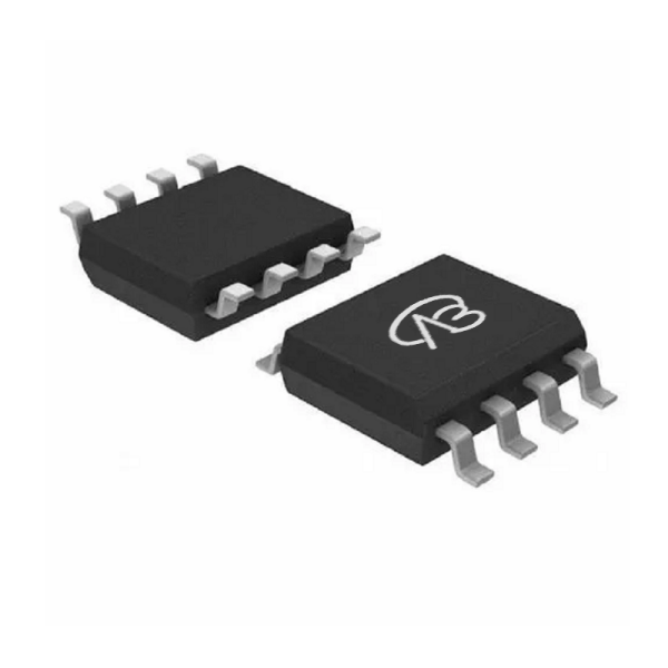
Product parameter:
| VB Package |
Configuration |
VDS(V) |
VGS |
Vthyp(V) |
ID(A) |
Rds2.5 |
Rds4.5 |
Rds10 |
Technology |
| SOP8 |
Dual-N+P |
±30V |
|
1.6/-1.7V |
±8A |
|
|
18/40mΩ |
Trench |
| VB Package |
Configuration |
VCE |
VGE |
VGEth(V) |
VCEsat15V |
ICE |
Technology |
| SOP8 |
Dual-N+P |
|
|
|
|
|
Trench |
| VB Package |
Configuration |
VDS(V) |
VGS |
Vthyp(V) |
ID(A) |
Rds18 |
Technology |
| SOP8 |
Dual-N+P |
±30V |
|
1.6/-1.7V |
±8A |
|
Trench |
| VB Package |
Configuration |
VDS(V) |
VGS |
Vthyp(V) |
ID(A) |
Rds6 |
Technology |
| SOP8 |
Dual-N+P |
±30V |
|
1.6/-1.7V |
±8A |
|
Trench |
| VB Package |
Polarity |
Vz / VR |
Pd |
VF |
IF |
IR |
Cd |
Type |
| SOP8 |
Dual-N+P |
|
|
|
|
|
|
|
Detailed parameter description
- **Package:** SOP8
- **Configuration:** Dual N-channel + P-channel
- **Drain-source voltage (VDS):** ±30V
- **Gate-source voltage (VGS):** ±20V
- **Threshold voltage (Vth):** 1.6V (N-channel) / -1.7V (P-channel)
- **On-resistance (RDS(ON)):**
- N-channel @ VGS = 4.5V: 24mΩ
- N-channel @ VGS = 10V: 18mΩ
- P-channel @ VGS = 4.5V: 50mΩ
- P-channel @ VGS = 10V: 40mΩ
- **Continuous drain current (ID):** ±8A
- **Technology:** Trench
The low on-resistance and high current capability of the GSS4501-VB MOSFET enable it to provide superior performance in a variety of applications, including high-efficiency switching and power management systems.
Domain and module applications:
Applications and module examples
1. **Power management system:**
GSS4501-VB is suitable for power management systems such as power switches and power distribution modules. Its dual MOSFET design enables it to efficiently handle power switching and regulation, especially in situations with high current loads and high efficiency requirements.
2. **DC-DC converter:**
In DC-DC converter modules, GSS4501-VB is able to provide efficient switching performance and is suitable for buck converters or boost converters. Its low RDS(ON) characteristics help improve overall conversion efficiency and reduce power losses, and is widely used in telecommunications equipment and consumer electronics.
3. **Motor drive circuit:**
The dual N-channel and P-channel configuration of this MOSFET makes it suitable for motor drive circuits. Whether it is a DC motor or a stepper motor, GSS4501-VB is able to provide stable performance in switching control and optimize the efficiency and response speed of the motor.
4. **Load Switch:**
In load switch applications, the GSS4501-VB can be used to achieve efficient load switching. Its dual MOSFET configuration allows simultaneous control of high-side and low-side switches, suitable for load management of various electronic devices, such as computer power supplies and home appliances.
By using the GSS4501-VB in these application areas, designers can ensure the efficiency and reliability of the equipment while meeting the stringent power and performance requirements of modern electronic systems.
* Please note: the above is only an example application scenario, the specific application depends on the requirements and conditions of the system design. When using this device, consult its data sheet for detailed technical specifications and features
Technical support:
* If you have any questions about the product, please fill out the form to submit, we will reply you within 24 hours


 Download now

 中文
中文 English
 Back to previous page