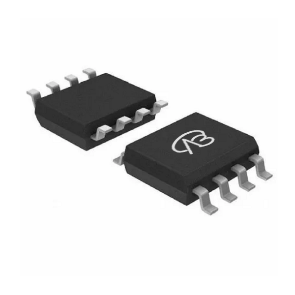
Product parameter:
| VB Package |
Configuration |
VDS(V) |
VGS |
Vthyp(V) |
ID(A) |
Rds2.5 |
Rds4.5 |
Rds10 |
Technology |
| SOP8 |
Dual-N+P |
±30V |
|
1.6/-1.7V |
±8A |
|
|
18/40mΩ |
Trench |
| VB Package |
Configuration |
VCE |
VGE |
VGEth(V) |
VCEsat15V |
ICE |
Technology |
| SOP8 |
Dual-N+P |
|
|
|
|
|
Trench |
| VB Package |
Configuration |
VDS(V) |
VGS |
Vthyp(V) |
ID(A) |
Rds18 |
Technology |
| SOP8 |
Dual-N+P |
±30V |
|
1.6/-1.7V |
±8A |
|
Trench |
| VB Package |
Configuration |
VDS(V) |
VGS |
Vthyp(V) |
ID(A) |
Rds6 |
Technology |
| SOP8 |
Dual-N+P |
±30V |
|
1.6/-1.7V |
±8A |
|
Trench |
| VB Package |
Polarity |
Vz / VR |
Pd |
VF |
IF |
IR |
Cd |
Type |
| SOP8 |
Dual-N+P |
|
|
|
|
|
|
|
2. FDS8960C-VB Detailed parameter description
- **Package type**: SOP8
- **Configuration**: Dual channel (N+P-channel)
- **Drain-source voltage (VDS)**: ±30V
- **Gate-source voltage (VGS)**: ±20V
- **Threshold voltage (Vth)**:
- N-channel: 1.6V
- P-channel: -1.7V
- **On-resistance (RDS(ON))**:
- N-channel: 24mΩ @ VGS=4.5V; 18mΩ @ VGS=10V
- P-channel: 50mΩ @ VGS=4.5V; 40mΩ @ VGS=10V
- **Maximum drain current (ID)**: ±8A
- **Technology**: Trench technology
- **Maximum power consumption**: Depends on specific application and thermal design.
Domain and module applications:
III. Application fields and module examples
1. **Power management system**: FDS8960C-VB is an ideal choice in power management systems, especially for circuits that require bipolar control. Its N+P dual-channel configuration allows for switching control of positive and negative voltages in the same package, providing flexible power distribution and management capabilities.
2. **Battery protection circuit**: This MOSFET has significant advantages in battery protection circuits. P-channel MOSFETs can be used for battery charge and discharge control, while N-channel MOSFETs can be used for overcurrent protection. Its low on-resistance and high current handling capabilities ensure the efficiency and safety of battery management systems.
3. **Load switch**: FDS8960C-VB performs well in load switch applications and can efficiently control various types of loads. Its bipolar design enables it to handle loads of different voltage polarities, suitable for a variety of complex load switching scenarios, such as applications in mobile devices and portable electronic devices.
4. **DC-DC Converter**: The dual-channel configuration of this device provides flexible design options in DC-DC converters, which can effectively manage the conversion of input and output voltages and improve the efficiency and stability of the converter.
In summary, the FDS8960C-VB is a high-performance bipolar MOSFET that is widely used in power management, battery protection, load switching, and DC-DC converters. It provides flexibility and efficient switch control capabilities for circuit design and is an important device in complex power management systems.
* Please note: the above is only an example application scenario, the specific application depends on the requirements and conditions of the system design. When using this device, consult its data sheet for detailed technical specifications and features
Technical support:
* If you have any questions about the product, please fill out the form to submit, we will reply you within 24 hours


 Download now

 中文
中文 English
 Back to previous page