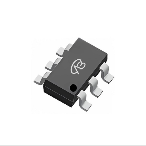
Product parameter:
| VB Package |
Configuration |
VDS(V) |
VGS |
Vthyp(V) |
ID(A) |
Rds2.5 |
Rds4.5 |
Rds10 |
Technology |
| SC70-6 |
Dual-N+P |
±20V |
|
1.0/-1.2V |
3.28/-2.8A |
110/190mΩ |
|
|
Trench |
| VB Package |
Configuration |
VCE |
VGE |
VGEth(V) |
VCEsat15V |
ICE |
Technology |
| SC70-6 |
Dual-N+P |
|
|
|
|
|
Trench |
| VB Package |
Configuration |
VDS(V) |
VGS |
Vthyp(V) |
ID(A) |
Rds18 |
Technology |
| SC70-6 |
Dual-N+P |
±20V |
|
1.0/-1.2V |
3.28/-2.8A |
|
Trench |
| VB Package |
Configuration |
VDS(V) |
VGS |
Vthyp(V) |
ID(A) |
Rds6 |
Technology |
| SC70-6 |
Dual-N+P |
±20V |
|
1.0/-1.2V |
3.28/-2.8A |
|
Trench |
| VB Package |
Polarity |
Vz / VR |
Pd |
VF |
IF |
IR |
Cd |
Type |
| SC70-6 |
Dual-N+P |
|
|
|
|
|
|
|
Detailed parameter description
- **Package:** SC70-6
- **Configuration:** Dual N-Channel + P-Channel
- **Drain-source voltage (VDS):** ±20V
- **Gate-source voltage (VGS):** ±20V
- **Threshold voltage (Vth):**
- N-Channel: 1.0V
- P-Channel: -1.2V
- **On-resistance (RDS(ON)):**
- N-Channel:
- 110mΩ @ VGS = 2.5V
- 90mΩ @ VGS = 4.5V
- P-Channel:
- 190mΩ @ VGS = 2.5V
- 155mΩ @ VGS = 4.5V
- **Continuous leakage current (ID):**
- N-Channel: 3.28A
- P-Channel: -2.8A
- **Technology:** Trench
Domain and module applications:
Applications and module examples
1. **Power management:** The FDG6320C-VB is ideal for use in power management systems such as DC-DC converters and power switching circuits. Its dual MOSFET configuration allows both positive and negative power switching to be handled on the same chip, improving the compactness and efficiency of circuit design.
2. **Load switch:** Due to its low on-resistance and high current capability, the FDG6320C-VB is suitable for high-efficiency load switching applications. It can efficiently switch load currents in small devices and is suitable for use in switch modules in consumer electronics and industrial equipment.
3. **Battery protection:** In battery management systems, the FDG6320C-VB can be used to protect batteries from overcurrent and overvoltage. The dual MOSFET configuration enables bidirectional protection, ensuring safe use of the battery and improving system reliability.
4. **LED drive:** The device is suitable for use in LED drive circuits because its low on-resistance and compact package help improve the efficiency of the drive current. FDG6320C-VB can effectively control the current in the LED driver module to ensure the stability and brightness of the LED.
The dual MOSFET configuration, low on-resistance and compact SC70-6 package of FDG6320C-VB make it an ideal choice for applications that require high efficiency and miniaturization, especially in power management and switching applications.
* Please note: the above is only an example application scenario, the specific application depends on the requirements and conditions of the system design. When using this device, consult its data sheet for detailed technical specifications and features
Technical support:
* If you have any questions about the product, please fill out the form to submit, we will reply you within 24 hours


 Download now

 中文
中文 English
 Back to previous page